
FIGURE 10. 1
VLSI Implementation of Parwan, Fabricated at Massachusetts Microelectronics Center.

FIGURE 10. 2
Page and Offset Parts of Parwan addresses.
|
Instruction Mnemonic |
Brief Description |
Address Bits |
Address Scheme |
Indirect Address |
Flags Use |
Flags Set |
|
LDA loc |
Load AC w/(loc) |
12 |
FULL |
YES |
---- |
--zn |
|
AND loc |
AND AC w/(loc) |
12 |
FULL |
YES |
---- |
--zn |
|
ADD loc |
Add (loc) to AC |
12 |
FULL |
YES |
-c-- |
vczn |
|
SUB loc |
Sub (loc) from AC |
12 |
FULL |
YES |
-c-- |
vczn |
|
JMP adr |
Jump to adr |
12 |
FULL |
YES |
---- |
---- |
|
STA loc |
Store AC in loc |
12 |
FULL |
YES |
---- |
---- |
|
JSR tos |
Subroutine to tos |
8 |
PAGE |
NO |
---- |
---- |
|
BRA_V adr |
Branch to adr if V |
8 |
PAGE |
NO |
v--- |
---- |
|
BRA_C adr |
Branch to adr if C |
8 |
PAGE |
NO |
-c-- |
---- |
|
BRA_Z adr |
Branch to adr if Z |
8 |
PAGE |
NO |
--z- |
---- |
|
BRA_N adr |
Branch to adr if N |
8 |
PAGE |
NO |
---n |
---- |
|
NOP |
No operation |
- |
NONE |
NO |
---- |
---- |
|
CLA |
Clear AC |
- |
NONE |
NO |
---- |
---- |
|
CMA |
Complement AC |
- |
NONE |
NO |
---- |
--zn |
|
CMC |
Complement carry |
- |
NONE |
NO |
-c-- |
-c-- |
|
ASL |
Arith shift left |
- |
NONE |
NO |
---- |
vczn |
|
ASR |
Arith shift right |
- |
NONE |
NO |
---- |
--zn |
FIGURE 10. 3
Summary of Parwan instructions.
|
Instruction Mnemonic |
Opcode Bits 7 6 5 |
D/I Bit 4 |
Bits 3 2 1 0 |
|
LDA loc |
0 0 0 |
0/1 |
Page adr |
|
AND loc |
0 0 1 |
0/1 |
Page adr |
|
ADD loc |
0 1 0 |
0/1 |
Page adr |
|
SUB loc |
0 1 1 |
0/1 |
Page adr |
|
JMP adr |
1 0 0 |
0/1 |
Page adr |
|
STA loc |
1 0 1 |
0/1 |
Page adr |
|
JSR tos |
1 1 0 |
- |
- - - - |
|
BRA_V adr |
1 1 1 |
1 |
1 0 0 0 |
|
BRA_C adr |
1 1 1 |
1 |
0 1 0 0 |
|
BRA_Z adr |
1 1 1 |
1 |
0 0 1 0 |
|
BRA_N adr |
1 1 1 |
1 |
0 0 0 1 |
|
NOP |
1 1 1 |
0 |
0 0 0 0 |
|
CLA |
1 1 1 |
0 |
0 0 0 1 |
|
CMA |
1 1 1 |
0 |
0 0 1 0 |
|
CMC |
1 1 1 |
0 |
0 1 0 0 |
|
ASL |
1 1 1 |
0 |
1 0 0 0 |
|
ASR |
1 1 1 |
0 |
1 0 0 1 |
FIGURE 10. 4
Parwan instruction opcodes.

FIGURE 10. 5
Addressing in full-address instructions.
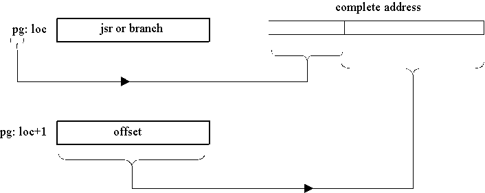
FIGURE 10. 6
Addressing in page-address instructions.
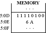
FIGURE 10. 7
A branch instruction.
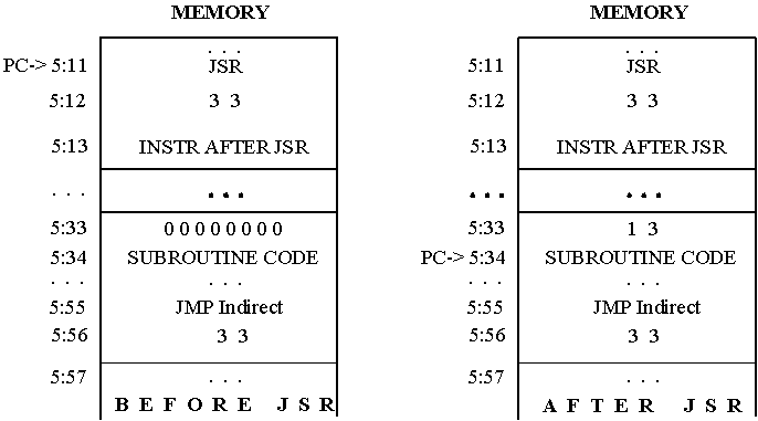
FIGURE 10. 8
An example for the execution of jsr. Memory and pc, before and after jsr.

FIGURE 10. 9
An example for indirect addressing in Parwan.
-- load 25 in 4:00
-- load 10 in 4:01
-- load 01 in 4:02
0:15 cla -- clear accumulator
0:16 asl -- clears carry
0:17 add, i 4:00 -- add bytes
0:19 sta 4:03 -- store partial sum
0:1B lda 4:00 -- load pointer
0:1D add 4:02 -- increment pointer
0:1F sta 4:00 -- store pointer back
0:21 lda 4:01 -- load count
0:23 sub 4:02 -- decrement count
0:25 bra_z :2D -- end if zero count
0:27 sta 4:01 -- store count back
0:29 lda 4:03 -- get partial sum
0:2B jmp 0:17 -- go for next byte
0:2D nop -- adding completed
FIGURE 10. 10
An example program for Parwan CPU.
LIBRARY cmos;
USE cmos.basic_utilities.ALL;
--
PACKAGE par_utilities IS
FUNCTION "XOR" (a, b : qit) RETURN qit ;
FUNCTION "AND" (a, b : qit_vector) RETURN qit_vector;
FUNCTION "OR" (a, b : qit_vector) RETURN qit_vector;
FUNCTION "NOT" (a : qit_vector) RETURN qit_vector;
--
SUBTYPE nibble IS qit_vector (3 DOWNTO 0);
SUBTYPE byte IS qit_vector (7 DOWNTO 0);
SUBTYPE twelve IS qit_vector (11 DOWNTO 0);
--
SUBTYPE wired_nibble IS wired_qit_vector (3 DOWNTO 0);
SUBTYPE wired_byte IS wired_qit_vector (7 DOWNTO 0);
SUBTYPE wired_twelve IS wired_qit_vector (11 DOWNTO 0);
--
SUBTYPE ored_nibble IS ored_qit_vector (3 DOWNTO 0);
SUBTYPE ored_byte IS ored_qit_vector (7 DOWNTO 0);
SUBTYPE ored_twelve IS ored_qit_vector (11 DOWNTO 0);
--
CONSTANT zero_4 : nibble := "0000";
CONSTANT zero_8 : byte := "00000000";
CONSTANT zero_12 : twelve := "000000000000";
--
FUNCTION add_cv (a, b : qit_vector; cin : qit) RETURN qit_vector;
FUNCTION sub_cv (a, b : qit_vector; cin : qit) RETURN qit_vector;
--
FUNCTION set_if_zero (a : qit_vector) RETURN qit;
--
END par_utilities;
FIGURE 10. 11
Declarations of par_utilities package of par_library.
PACKAGE BODY par_utilities IS FUNCTION "XOR" (a, b : qit) RETURN qit IS
CONSTANT qit_xor_table : qit_2d := (
('0','1','1','X'),
('1','0','0','X'),
('1','0','0','X'),
('X','X','X','X'));
BEGIN
RETURN qit_xor_table (a, b);
END "XOR";
FUNCTION "AND" (a,b : qit_vector) RETURN qit_vector IS
VARIABLE r : qit_vector (a'RANGE);
BEGIN
loop1: FOR i IN a'RANGE LOOP
r(i) := a(i) AND b(i);
END LOOP loop1;
RETURN r;
END "AND";
--
FUNCTION "OR" (a,b: qit_vector) RETURN qit_vector IS
VARIABLE r: qit_vector (a'RANGE);
BEGIN
loop1: FOR i IN a'RANGE LOOP
r(i) := a(i) OR b(i);
END LOOP loop1;
RETURN r;
END "OR";
--
FUNCTION "NOT" (a: qit_vector) RETURN qit_vector IS
VARIABLE r: qit_vector (a'RANGE);
BEGIN
loop1: FOR i IN a'RANGE LOOP
r(i) := NOT a(i);
END LOOP loop1;
RETURN r;
END "NOT";
FIGURE 10. 12
Body of par_utilities package of par_library library. (continued on following page)
FUNCTION add_cv (a, b : qit_vector; cin : qit) RETURN qit_vector IS VARIABLE r, c: qit_vector (a'LEFT + 2 DOWNTO 0);
-- extra r bits : msb: overflow, next to msb: carry
VARIABLE a_sign, b_sign: qit; BEGIN a_sign := a(a'LEFT);
b_sign := b(b'LEFT);
r(0) := a(0) XOR b(0) XOR cin;
c(0) := ((a(0) XOR b(0)) AND cin) OR (a(0) AND b(0));
FOR i IN 1 TO (a'LEFT) LOOP
r(i) := a(i) XOR b(i) XOR c(i-1);
c(i) := ((a(i) XOR b(i)) AND c(i-1)) OR (a(i) AND b(i));
END LOOP;
r(a'LEFT+1) := c(a'LEFT);
IF a_sign = b_sign AND r(a'LEFT) /= a_sign THEN
r(a'LEFT+2) := '1'; --overflow
ELSE
r(a'LEFT+2) := '0';
END IF;
RETURN r;
END add_cv;
FUNCTION sub_cv (a, b : qit_vector; cin : qit) RETURN qit_vector IS
VARIABLE not_b : qit_vector (b'LEFT DOWNTO 0);
VARIABLE not_c : qit;
VARIABLE r : qit_vector (a'LEFT + 2 DOWNTO 0);
BEGIN
not_b := NOT b;
not_c := NOT cin;
r := add_cv (a, not_b, not_c);
RETURN r;
END sub_cv;
FUNCTION set_if_zero (a : qit_vector) RETURN qit IS
VARIABLE zero : qit := '1';
BEGIN
FOR i IN a'RANGE LOOP
IF a(i) /= '0'
THEN zero := '0'; EXIT;
END IF;
END LOOP;
RETURN zero;
END set_if_zero;
END par_utilities;
FIGURE 10.12
Body of the par_utilities package of par_library library. (continued from previous page)
LIBRARY cmos;USE cmos.basic_utilities.ALL;--PACKAGE par_parameters IS CONSTANT single_byte_instructions : qit_vector (3 DOWNTO 0) := "1110"; CONSTANT cla : qit_vector (3 DOWNTO 0) := "0001";
CONSTANT cma : qit_vector (3 DOWNTO 0) := "0010";
CONSTANT cmc : qit_vector (3 DOWNTO 0) := "0100";
CONSTANT asl : qit_vector (3 DOWNTO 0) := "1000";
CONSTANT asr : qit_vector (3 DOWNTO 0) := "1001";
CONSTANT jsr : qit_vector (2 DOWNTO 0) := "110";
CONSTANT bra : qit_vector (3 DOWNTO 0) := "1111";
CONSTANT indirect : qit := '1';
CONSTANT jmp : qit_vector (2 DOWNTO 0) := "100";
CONSTANT sta : qit_vector (2 DOWNTO 0) := "101";
CONSTANT lda : qit_vector (2 DOWNTO 0) := "000";
CONSTANT ann : qit_vector (2 DOWNTO 0) := "001";
CONSTANT add : qit_vector (2 DOWNTO 0) := "010";
CONSTANT sbb : qit_vector (2 DOWNTO 0) := "011";
CONSTANT jsr_or_bra : qit_vector (1 DOWNTO 0) := "11";
END par_parameters;
FIGURE 10. 13
Declaration of par_parameters Package of par_library.
LIBRARY cmos;USE cmos.basic_utilities.ALL;--
LIBRARY par_library;USE par_library.par_utilities.ALL;USE par_library.par_parameters.ALL;--ENTITY par_central_processing_unit IS GENERIC (read_high_time, read_low_time,
write_high_time, write_low_time : TIME := 2 US;
cycle_time : TIME := 4 US);
PORT (clk : IN qit;
interrupt : IN qit;
read_mem, write_mem : OUT qit;
databus : INOUT wired_byte BUS := "ZZZZZZZZ"; adbus : OUT twelve
);
END par_central_processing_unit;
FIGURE 10. 14
Interface description of Parwan.
ARCHITECTURE behavioral OF par_central_processing_unit ISBEGIN PROCESS Declare necessary variables; Figure 10.16. BEGIN IF interrupt = '1' THEN Handle interrupt; Figure 10.17.
ELSE -- no interrupt
Read first byte into byte1, increment pc; Figure 10.18.
IF byte1 (7 DOWNTO 4) = single_byte_instructions THEN
Execute single-byte instructions; Figure 10.19.
ELSE -- two-byte instructions
Read second byte into byte2, increment pc; Figure 10.20.
IF byte1 (7 DOWNTO 5) = jsr THEN
Execute jsr instruction, byte2 has address; Figure 10.21.
ELSIF byte1 (7 DOWNTO 4) = bra THEN
Execute bra instructions, address in byte2; Figure 10.22.
ELSE -- all other two-byte instructions
IF byte1 (4) = indirect THEN
Use byte1 and byte2 to get address; Figure 10.23.
END IF; -- ends indirect
IF byte1 (7 DOWNTO 5) = jmp THEN
Execute jmp instruction; Figure 10.24;
ELSIF byte1 (7 DOWNTO 5) = sta THEN
Execute sta instruction, write ac; Figure 10.25.
ELSE -- read operand for lda, and, add, sub
Read memory onto databus; Figure 10.26, top.
Execute lda, and, add, and sub; Figure 10.26, middle.
Remove memory from databus; Figure 10.26, bottom.
END IF; -- jmp / sta / lda, and, add, sub
END IF; -- jsr / bra / other double-byte instructions
END IF; -- single-byte / double-byte
END IF; -- interrupt / otherwise
END PROCESS;
END behavioral;
FIGURE 10. 15
Outline of the Behavioral Description of Parwan.
VARIABLE pc : twelve;VARIABLE ac, byte1, byte2 : byte;VARIABLE v, c, z, n : qit;VARIABLE temp : qit_vector (9 DOWNTO 0);
FIGURE 10. 16
Variable declarations of Parwan behavioral model.
pc := zero_12;WAIT FOR cycle_time;
FIGURE 10. 17
Interrupt handling of Parwan behavioral model.
adbus <= pc;read_mem <= '1'; WAIT FOR read_high_time;byte1 := byte (databus);read_mem <= '0'; WAIT FOR read_low_time;pc := inc (pc);
FIGURE 10. 18
Reading the first byte from the memory, part of Parwan behavioral model.
CASE byte1 (3 DOWNTO 0) ISWHEN cla => ac := zero_8;WHEN cma => ac := NOT ac;
IF ac = zero_8 THEN z := '1'; END IF;
n := ac (7);
WHEN cmc =>
c := NOT c;
WHEN asl =>
c := ac (7);
ac := ac (6 DOWNTO 0) & '0';
IF ac = zero_8 THEN z := ‘1’; END IF;
n := ac (7);
IF c /= n THEN v := '1'; END IF;
WHEN asr =>
ac := ac (7) & ac (7 DOWNTO 1);
IF ac = zero_8 THEN z := '1'; END IF;
n := ac (7);
WHEN OTHERS => NULL;
END CASE;
FIGURE 10. 19
Executing single-byte instructions in the behavioral model of Parwan.
adbus <= pc;read_mem <= '1'; WAIT FOR read_high_time;byte2 := byte (databus);read_mem <= '0'; WAIT FOR read_low_time;pc := inc (pc);
FIGURE 10. 20
Reading the second byte from the memory, part of Parwan behavioral model.
databus <= wired_byte (pc (7 DOWNTO 0) );adbus (7 DOWNTO 0) <= byte2;
write_mem <= '1'; WAIT FOR write_high_time;
write_mem <= '0'; WAIT FOR write_low_time;
databus <= "ZZZZZZZZ";
pc (7 DOWNTO 0) := inc (byte2);
FIGURE 10. 21
Execution of the jsr instruction in the behavioral model of Parwan.
IF ( byte1 (3) = '1' AND v = '1' ) OR ( byte1 (2) = '1' AND c = '1' ) OR ( byte1 (1) = '1' AND z = '1' ) OR ( byte1 (0) = '1' AND n = '1' )
THEN
pc (7 DOWNTO 0) := byte2;
END IF;
FIGURE 10. 22
Execution of branch instructions in the behavioral model of Parwan.
adbus (11 DOWNTO 8) <= byte1 (3 DOWNTO 0);adbus (7 DOWNTO 0) <= byte2;read_mem <= '1'; WAIT FOR read_high_time;byte2 := byte (databus);read_mem <= '0'; WAIT FOR read_low_time;
FIGURE 10. 23
Handling indirect addressing by the behavioral model of Parwan.
pc := byte1 (3 DOWNTO 0) & byte2;
FIGURE 10. 24
Execution of jmp instruction in the behavioral model of Parwan.
adbus <= byte1 (3 DOWNTO 0) & byte2;databus <= wired_byte (ac);write_mem <= '1'; WAIT FOR write_high_time;
write_mem <= '0'; WAIT FOR write_low_time;
databus <= "ZZZZZZZZ";
FIGURE 10. 25
Execution of sta instruction in the behavioral model of Parwan.
adbus (11 DOWNTO 8) <= byte1 (3 DOWNTO 0);
adbus (7 DOWNTO 0) <= byte2;
read_mem <= '1'; WAIT FOR read_high_time;
CASE byte1 (7 DOWNTO 5) IS
WHEN lda =>
ac := byte (databus);
WHEN ann =>
ac := ac AND byte (databus);
WHEN add =>
temp := add_cv (ac, byte (databus), c);
ac := temp (7 DOWNTO 0);
c := temp (8);
v := temp (9);
WHEN sbb =>
temp := sub_cv (ac, byte (databus), c);
ac := temp (7 DOWNTO 0);
c := temp (8);
v := temp (9);
WHEN OTHERS => NULL;
END CASE;
IF ac = zero_8 THEN z := '1'; END IF;
n := ac (7);
read_mem <= '0'; WAIT FOR read_low_time;
FIGURE 10. 26
Execution of lda, and, add, and sub instructions in the behavioral model of Parwan.

FIGURE 10. 27
Bussing structure of Parwan.
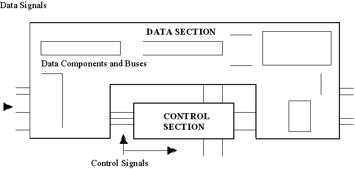
FIGURE 10. 28
Data and control sections of Parwan CPU.
|
Applies To |
Category |
Signal Name |
Functionality |
|
AC |
Register Control |
load_ac, zero_ac |
Loads ac Resets ac |
|
IR |
Register Control |
load_ir |
Loads ir |
|
PC |
Register Control |
increment_pc, load_page_pc, load_offset_pc, reset_pc |
Increments pc Loads page part of pc Loads offset part of pc Resets pc |
|
MAR |
Register Control |
load_page_mar, load_offset_mar |
Loads page part of mar Loads offset part of mar |
|
SR |
Register Control |
load_sr, cm_carry_sr |
Loads sr Complements carry flag of sr |
|
|
|
|
|
|
MAR_BUS |
Bus Control |
pc_on_mar_page_bus, ir_on_mar_page_bus, pc_on_mar_offset_bus, dbus_on_mar_offset_bus |
Puts page part of pc on mar page bus Puts 4 bits of ir on mar page bus Puts offset part of pc on mar offset bus Puts dbus on mar offset bus |
|
DBUS |
Bus Control |
pc_offset_on_dbus, obus_on_dbus, databus_on_dbus |
Puts offset part of pc on dbus Puts obus on dbus Puts external databus on internal dbus |
|
ADBUS |
Bus Control |
mar_on_adbus |
Puts all of mar on adbus |
|
DATABUS |
Bus Control |
dbus_on_databus |
Puts internal dbus on external databus |
|
|
|
||
|
SHU |
Logic Units |
arith_shift_left, arith_shift_right |
Shifter shifts its input one place to the left Shifter shifts its input one place to the right |
|
ALU |
Logic Units |
alu_and, alu_not, alu_a, alu_add, alu_b, alu_sub |
Output of alu becomes and of its two inputs Output of alu becomes complement of its b input Output of alu becomes the same as its a input alu perfporms add operation on its two inputs Output of alu becomes the same as its b input alu perfporms subtraction of its two inputs |
|
Others |
I/O |
read_mem, write_mem, interrupt |
Starts a memory read operation Starts a memory write operation Interrupts CPU |
FIGURE 10. 29
Inputs and outputs of Parwan control section

FIGURE 10. 30
Timing of control signals.
|
Id |
Opcode line |
Operation |
Flags |
|
0 |
alu_and |
a AND b |
zn |
|
1 |
alu_not |
NOT b |
zn |
|
2 |
alu_a |
a |
zn |
|
3 |
alu_add |
b PLUS a |
vczn |
|
4 |
alu_b |
b |
zn |
|
5 |
alu_sub |
b MINUS a |
vczn |
FIGURE 10. 31
Operations and flags of alu.


FIGURE 10. 32
Parwan alu. (a) Logic symbol, (b) one bit gate level hardware.
LIBRARY cmos;USE cmos.basic_utilities.ALL;
--PACKAGE alu_operations IS CONSTANT a_and_b : qit_vector (5 DOWNTO 0) := "000001"; CONSTANT b_compl : qit_vector (5 DOWNTO 0) := "000010";
CONSTANT a_input : qit_vector (5 DOWNTO 0) := "000100";
CONSTANT a_add_b : qit_vector (5 DOWNTO 0) := "001000";
CONSTANT b_input : qit_vector (5 DOWNTO 0) := "010000";
CONSTANT a_sub_b : qit_vector (5 DOWNTO 0) := "100000";
END alu_operations;
FIGURE 10. 33
Package declaration for the alu_operations package.
ENTITY arithmetic_logic_unit IS PORT (a_side, b_side : IN byte;
alu_and, alu_not, alu_a, alu_add, alu_b, alu_sub : IN qit; in_flags : IN nibble; z_out : OUT byte; out_flags : OUT nibble);END arithmetic_logic_unit;--ARCHITECTURE behavioral OF arithmetic_logic_unit IS
BEGIN
coding: PROCESS (a_side, b_side, alu_and, alu_not, alu_a, alu_add, alu_b, alu_sub)
VARIABLE t : qit_vector (9 DOWNTO 0);
VARIABLE v, c, z, n : qit;
ALIAS n_flag_in : qit IS in_flags(0);
ALIAS z_flag_in : qit IS in_flags(1);
ALIAS c_flag_in : qit IS in_flags(2);
ALIAS v_flag_in : qit IS in_flags(3);
BEGIN
CASE qit_vector (5 DOWNTO 0)’ (alu_sub, alu_b, alu_add, alu_a, alu_not, alu_and) IS
WHEN a_add_b =>
t := add_cv (b_side, a_side, c_flag_in);
c := t(8); v := t(9); -- other flags are set at the end
WHEN a_sub_b =>
t := sub_cv (b_side, a_side, c_flag_in);
c := t(8); v := t(9);
WHEN a_and_b =>
t (7 DOWNTO 0) := a_side AND b_side;
c := c_flag_in; v := v_flag_in;
WHEN a_input =>
t (7 DOWNTO 0) := a_side;
c := c_flag_in; v := v_flag_in;
WHEN b_input =>
t (7 DOWNTO 0) := b_side;
c := c_flag_in; v := v_flag_in;
WHEN b_compl =>
t (7 DOWNTO 0) := NOT b_side;
c := c_flag_in; v := v_flag_in;
WHEN OTHERS => NULL;
END CASE;
n := t(7);
z := set_if_zero (t (7 DOWNTO 0));
z_out <= t (7 DOWNTO 0);
out_flags <= (v, c, z, n);
END PROCESS coding;
END behavioral;
FIGURE 10. 34
Behavioral description of arithmetic logic unit of Parwan.


FIGURE 10. 35
Parwan shu. (a) Logic symbol, (b) one bit hardware.
ENTITY shifter_unit IS PORT (alu_side : IN byte; arith_shift_left, arith_shift_right : IN qit; in_flags : IN nibble; obus_side : OUT byte; out_flags : OUT nibble);
END shifter_unit;
--
ARCHITECTURE behavioral OF shifter_unit IS
BEGIN
coding: PROCESS (alu_side, arith_shift_left, arith_shift_right)
VARIABLE t : qit_vector (7 DOWNTO 0);
VARIABLE v, c, z, n : qit;
ALIAS n_flag_in : qit IS in_flags(0);
ALIAS z_flag_in : qit IS in_flags(1);
ALIAS c_flag_in : qit IS in_flags(2);
ALIAS v_flag_in : qit IS in_flags(3);
BEGIN
IF arith_shift_right = '0' AND arith_shift_left = '0' THEN
t := alu_side (7 DOWNTO 0);
(v, c, z, n) := in_flags; ELSIF arith_shift_left = '1' THEN t := alu_side (6 DOWNTO 0) & '0'; n := t (7); z := set_if_zero (t);
c := alu_side (7);
v := alu_side (6) XOR alu_side (7);
ELSIF arith_shift_right = '1' THEN
t := alu_side (7) & alu_side (7 DOWNTO 1);
n := t (7);
z := set_if_zero (t);
c := c_flag_in;
v := v_flag_in;
END IF;
obus_side <= t;
out_flags <= (v, c, z, n);
END PROCESS coding;
END behavioral;
FIGURE 10. 36
Behavioral Description of the Shifter Unit of Parwan.


FIGURE 10. 37
The status register. (a) Logic symbol, (b) one bit hardware.
ENTITY status_register_unit IS PORT (in_flags : IN nibble; out_status : OUT nibble; load, cm_carry, ck : IN qit );END status_register_unit;
--
ARCHITECTURE behavioral OF status_register_unit IS
BEGIN
PROCESS (ck)
VARIABLE internal_state : nibble := "0000";
ALIAS internal_c : qit IS internal_state (2);
BEGIN
IF (ck = '0') THEN
IF (load = '1') THEN
internal_state := in_flags;
ELSIF (cm_carry = '1') THEN
internal_c := NOT internal_c;
END IF;
out_status <= internal_state;
END IF;
END PROCESS;
END behavioral;
FIGURE 10. 38
Behavioral description of the status register of Parwan.
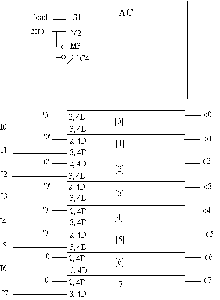
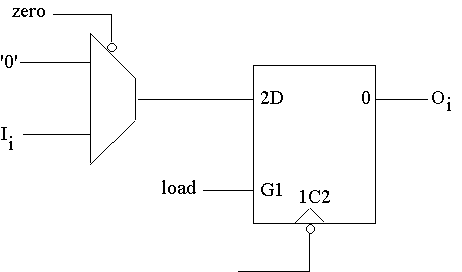
FIGURE 10. 39
Parwan accumulator, (a) Logic symbol, (b) one bit hardware.
ENTITY accumulator_unit IS PORT (i8 : IN byte; o8 : OUT byte; load, zero, ck : IN qit);
END accumulator_unit;
--
ARCHITECTURE dataflow OF accumulator_unit IS
BEGIN
enable : BLOCK (load = '1')
BEGIN
clocking : BLOCK ( (ck = '0' AND NOT ck'STABLE) AND GUARD )
BEGIN
o8 <= GUARDED "00000000" WHEN zero = '1' ELSE i8;
END BLOCK clocking;
END BLOCK enable;
END dataflow;
FIGURE 10. 40
Dataflow description of Parwan accumulator.


FIGURE 10. 41
The Parwan instruction, (a) Logic symbol, (b) one bit hardware.
ENTITY instruction_register_unit IS
PORT (i8 : IN byte; o8 : OUT byte; load, ck : IN qit);
END instruction_register_unit;
--
ARCHITECTURE dataflow OF instruction_register_unit IS
BEGIN
enable : BLOCK (load = '1')
BEGIN
clocking : BLOCK ( (ck = '0' AND NOT ck'STABLE) AND GUARD )
BEGIN
o8 <= GUARDED i8;
END BLOCK clocking;
END BLOCK enable;
END dataflow;
FIGURE 10. 42
Dataflow description of the instruction register of Parwan.


FIGURE 10. 43
Parwan program counter, (a) Logic symbol, (b) one bit hardware.
ENTITY program_counter_unit IS
PORT (i12 : IN twelve; o12 : OUT twelve;
increment, load_page, load_offset, reset, ck : IN qit);
END program_counter_unit;
--
ARCHITECTURE behavioral OF program_counter_unit IS
BEGIN
PROCESS (ck)
VARIABLE internal_state : twelve := zero_12;
BEGIN
IF (ck = '0' ) THEN
IF reset = '1' THEN
internal_state := zero_12;
ELSIF increment = '1' THEN
internal_state := inc (internal_state);
ELSE
IF load_page = '1' THEN
internal_state (11 DOWNTO 8) := i12 (11 DOWNTO 8);
END IF;
IF load_offset = '1' THEN
internal_state (7 DOWNTO 0) := i12 (7 DOWNTO 0);
END IF;
END IF;
o12 <= internal_state;
END IF;
END PROCESS;
END behavioral;
FIGURE 10. 44
Behavioral description of the program counter of Parwan.


FIGURE 10. 45
Logic symbol for the memory address register of Parwan.
ENTITY memory_address_register_unit IS
PORT (i12 : IN twelve; o12 : OUT twelve;
load_page, load_offset, ck : IN qit);
END memory_address_register_unit;
--
ARCHITECTURE behavioral OF memory_address_register_unit IS
BEGIN
PROCESS (ck)
VARIABLE internal_state : twelve := zero_12;
BEGIN
IF (ck = '0' ) THEN
IF load_page = '1' THEN
internal_state (11 DOWNTO 8) := i12 (11 DOWNTO 8);
END IF;
IF load_offset = '1' THEN
internal_state (7 DOWNTO 0) := i12 (7 DOWNTO 0);
END IF;
o12 <= internal_state;
END IF;
END PROCESS;
END behavioral;
FIGURE 10. 46
Behavioral description of the memory address register of Parwan.
ENTITY par_data_path IS
PORT (databus : INOUT wired_byte BUS := "ZZZZZZZZ"; adbus : OUT twelve;
clk : IN qit;
-- register controls:
load_ac, zero_ac,
load_ir,
increment_pc, load_page_pc, load_offset_pc, reset_pc,
load_page_mar, load_offset_mar,
load_sr, cm_carry_sr,
-- bus connections:
pc_on_mar_page_bus, ir_on_mar_page_bus,
pc_on_mar_offset_bus, dbus_on_mar_offset_bus,
pc_offset_on_dbus, obus_on_dbus, databus_on_dbus,
mar_on_adbus,
dbus_on_databus,
-- logic unit function control inputs:
arith_shift_left, arith_shift_right,
alu_and, alu_not, alu_a, alu_add, alu_b, alu_sub : IN qit;
-- outputs to the controller:
ir_lines : OUT byte; status : OUT nibble
);
END par_data_path;
FIGURE 10. 47
Entity Declaration of the Data Section of Parwan.
ARCHITECTURE structural OF par_data_path IS
--
COMPONENT ac
PORT (i8: IN byte; o8: OUT byte; load, zero, ck: IN qit);
END COMPONENT;
FOR r1: ac USE ENTITY WORK.accumulator_unit (dataflow);
--
COMPONENT ir
PORT (i8: IN byte; o8: OUT byte; load, ck: IN qit);
END COMPONENT;
FOR r2: ir USE ENTITY WORK.instruction_register_unit (dataflow);
--
COMPONENT pc
PORT (i12 : IN twelve; o12 : OUT twelve;
increment, load_page, load_offset, reset, ck : IN qit);
END COMPONENT;
FOR r3: pc USE ENTITY WORK.program_counter_unit (behavioral);
--
COMPONENT mar
PORT (i12 : IN twelve; o12 : OUT twelve; load_page, load_offset, ck : IN qit);
END COMPONENT;
FOR r4: mar USE ENTITY WORK.memory_address_register_unit (behavioral);
--
COMPONENT sr
PORT (in_flags : IN nibble; out_status : OUT nibble; load, cm_carry, ck : IN qit );
END COMPONENT;
FOR r5 : sr USE ENTITY WORK.status_register_unit (behavioral);
--
COMPONENT alu
PORT (a_side, b_side : IN byte; alu_and, alu_not, alu_a, alu_add, alu_b, alu_sub : IN qit;
in_flags : IN nibble; z_out : OUT byte; out_flags : OUT nibble);
END COMPONENT;
FOR l1 : alu USE ENTITY WORK.arithmetic_logic_unit (behavioral);
--
COMPONENT shu
PORT (alu_side : IN byte; arith_shift_left, arith_shift_right : IN qit;
in_flags : IN nibble; obus_side : OUT byte; out_flags : OUT nibble);
END COMPONENT;
FOR l2 : shu USE ENTITY WORK.shifter_unit (behavioral);
--
SIGNAL ac_out, ir_out, alu_out, obus : byte;
SIGNAL alu_a_inp : byte;
SIGNAL pc_out, mar_out : twelve;
SIGNAL dbus : wired_byte BUS;
SIGNAL alu_flags, shu_flags, sr_out : nibble;
SIGNAL mar_bus : wired_twelve BUS;
SIGNAL mar_inp : twelve;
FIGURE 10. 48
Declarative Part of the structural Architecture of par_data_path.
BEGIN
-- bus connections --
--
dbus1: alu_a_inp <= qit_vector (dbus);
dbus2: BLOCK (dbus_on_mar_offset_bus = '1')
BEGIN
mar_bus (7 DOWNTO 0) <= GUARDED dbus;
END BLOCK dbus2;
dbus3: BLOCK (dbus_on_databus = '1')
BEGIN
databus <= GUARDED dbus;
END BLOCK dbus3;
--
obus1: BLOCK (obus_on_dbus = '1')
BEGIN
dbus <= GUARDED wired_qit_vector (obus);
END BLOCK obus1;
--
databus1: BLOCK (databus_on_dbus = '1')
BEGIN
dbus <= GUARDED databus;
END BLOCK databus1;
--
mar_bus1: mar_inp <= qit_vector (mar_bus);
--
-- register connections --
--
r1: ac PORT MAP (obus, ac_out, load_ac, zero_ac, clk);
--
r2: ir PORT MAP (obus, ir_out, load_ir, clk);
ir1: ir_lines <= ir_out;
ir2: BLOCK (ir_on_mar_page_bus = '1')
BEGIN
mar_bus (11 DOWNTO 8) <= GUARDED wired_qit_vector (ir_out (3 DOWNTO 0));
END BLOCK ir2;
FIGURE 10. 49
Declarative part of the par_data_path structural Architecture. (continued on following page.)
r3: pc PORT MAP (mar_out, pc_out, increment_pc, load_page_pc, load_offset_pc, reset_pc, clk);
pc1: BLOCK (pc_on_mar_page_bus = '1')
BEGIN
mar_bus (11 DOWNTO 8) <= GUARDED wired_qit_vector (pc_out (11 DOWNTO 8));
END BLOCK pc1;
pc2: BLOCK (pc_on_mar_offset_bus = '1')
BEGIN
mar_bus (7 DOWNTO 0) <= GUARDED wired_qit_vector (pc_out (7 DOWNTO 0));
END BLOCK pc2;
pc3: BLOCK (pc_offset_on_dbus = '1')
BEGIN
dbus <= GUARDED wired_qit_vector (pc_out (7 DOWNTO 0));
END BLOCK pc3;
--
r4: mar PORT MAP (mar_inp, mar_out, load_page_mar, load_offset_mar, clk);
mar1: BLOCK (mar_on_adbus = '1')
BEGIN
adbus <= GUARDED mar_out;
END BLOCK mar1;
--
r5: sr PORT MAP (shu_flags, sr_out, load_sr, cm_carry_sr, clk);
sr1: status <= sr_out;
--
-- connection of logical and register structures --
--
l1: alu PORT MAP (alu_a_inp, ac_out, alu_and, alu_not, alu_a, alu_add, alu_b, alu_sub,
sr_out, alu_out, alu_flags);
l2: shu PORT MAP (alu_out, arith_shift_left, arith_shift_right, alu_flags, obus, shu_flags);
END structural;
FIGURE 10.49
Statement part of the par_data_path structural Architecture. (continued from previous page)
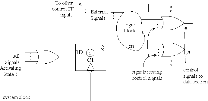
FIGURE 10. 50
Typical hardware surrounding a control flip-flop. The logic block in this figure is designated by a bubble.

FIGURE 10. 51
Example for the structure of Parwan control section.
ENTITY par_control_unit IS
GENERIC (read_delay, write_delay : TIME := 3 NS);
PORT (clk : IN qit;
-- register control signals:
load_ac, zero_ac,
load_ir,
increment_pc, load_page_pc, load_offset_pc, reset_pc,
load_page_mar, load_offset_mar,
load_sr, cm_carry_sr,
-- bus connection control signals:
pc_on_mar_page_bus, ir_on_mar_page_bus,
pc_on_mar_offset_bus, dbus_on_mar_offset_bus,
pc_offset_on_dbus, obus_on_dbus, databus_on_dbus,
mar_on_adbus,
dbus_on_databus,
-- logic unit function control outputs:
arith_shift_left, arith_shift_right, alu_and, alu_not, alu_a, alu_add, alu_b, alu_sub :
OUT ored_qit BUS;
-- inputs from the data section:
ir_lines : IN byte; status : IN nibble;
-- memory control and other external signals:
read_mem, write_mem : OUT ored_qit BUS; interrupt : IN qit
);
END par_control_unit;
FIGURE 10. 52
Entity declaration of Parwan control section.
ARCHITECTURE dataflow OF par_control_unit IS
SIGNAL s : ored_qit_vector (9 DOWNTO 1) REGISTER := "000000001";
BEGIN
FIGURE 10. 53
Declarative part of the par_control_unit dataflow architecture.
FIGURE 10. 54
Assigning signals with implied oring, par_control_unit outputs.
s1: BLOCK (s(1) = '1')
BEGIN -- start of fetch
-- pc to mar
pc_on_mar_page_bus <= GUARDED '1';
pc_on_mar_offset_bus <= GUARDED '1';
load_page_mar <= GUARDED '1';
load_offset_mar <= GUARDED '1';
-- reset pc if interrupt
reset_pc <= GUARDED '1' WHEN interrupt = '1' ELSE '0';
-- goto 2 if interrupt is off
ck: BLOCK ( (clk = '0' AND NOT clk'STABLE) AND GUARD )
BEGIN
s(1) <= GUARDED '1' WHEN interrupt = '1' ELSE '0';
s(2) <= GUARDED '1' WHEN interrupt /= '1' ELSE '0';
END BLOCK ck;
END BLOCK s1;

FIGURE 10. 55
State 1: starting a fetch, (a) VHDL code, (b) Hardware.
s2: BLOCK (s(2) = '1')
BEGIN -- fetching continues
-- read memory into ir
mar_on_adbus <= GUARDED '1';
read_mem <= GUARDED '1' AFTER read_delay;
databus_on_dbus <= GUARDED '1';
alu_a <= GUARDED ‘1’;
load_ir <= GUARDED '1';
-- increment pc
increment_pc <= GUARDED '1';
-- goto 3
ck: BLOCK ( (clk = '0' AND NOT clk'STABLE) AND GUARD )
BEGIN
s(3) <= GUARDED '1';
END BLOCK ck;
END BLOCK s2;
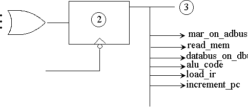
FIGURE 10. 56
State 2: completing a fetch, (a) VHDL code, (b) Hardware.
s3: BLOCK (s(3) = '1')
BEGIN
-- pc to mar, for next read
pc_on_mar_page_bus <= GUARDED '1';
pc_on_mar_offset_bus <= GUARDED '1';
load_page_mar <= GUARDED '1';
load_offset_mar <= GUARDED '1';
-- goto 4 if not single byte instruction
ck: BLOCK ( (clk = '0' AND NOT clk'STABLE) AND GUARD )
BEGIN
s(4) <= GUARDED '1' WHEN ir_lines (7 DOWNTO 4) /= "1110" ELSE '0';
END BLOCK ck;
-- perform single byte instructions
sb: BLOCK ( (ir_lines (7 DOWNTO 4) = "1110") AND GUARD)
BEGIN
(alu_not, alu_b) <= GUARDED
qit_vector’("10") WHEN ir_lines (1) = ‘1’ ELSE qit_vector’( "01");
arith_shift_left <= GUARDED
'1' WHEN ir_lines (3 DOWNTO 0) = "1000" ELSE '0';
arith_shift_right <= GUARDED
'1' WHEN ir_lines (3 DOWNTO 0) = "1001" ELSE '0';
load_sr <= GUARDED
'1' WHEN ( ir_lines (3) = '1' OR ir_lines (1) = '1' ) ELSE '0';
cm_carry_sr <= GUARDED '1' WHEN ir_lines (2) = '1' ELSE '0';
load_ac <= GUARDED
'1' WHEN ( ir_lines (3) = '1' OR ir_lines (1) = '1' ) ELSE '0';
zero_ac <= GUARDED
'1' WHEN ( ir_lines (3) = '0' AND ir_lines (0) = '1' ) ELSE '0';
ck: BLOCK ( (clk = '0' AND NOT clk'STABLE) AND GUARD )
BEGIN
s(2) <= GUARDED '1';
END BLOCK ck;
END BLOCK sb;
END BLOCK s3;
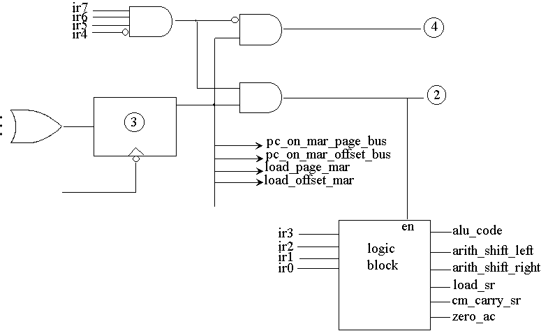
FIGURE 10. 57
State 3: preparing for address fetch, execution of single byte instructions, (a) VHDL code, (b) Hardware.
s4: BLOCK (s(4) = '1')
BEGIN -- page from ir, and offset from next memory makeup 12-bit address
-- read memory into mar offset
mar_on_adbus <= GUARDED '1';
read_mem <= GUARDED '1' AFTER read_delay;
databus_on_dbus <= GUARDED '1';
dbus_on_mar_offset_bus <= GUARDED '1';
load_offset_mar <= GUARDED '1'; -- completed operand (dir/indir) address
-- page from ir if not branch or jsr
pg: BLOCK ( (ir_lines (7 DOWNTO 6) /= "11") AND GUARD)
BEGIN
ir_on_mar_page_bus <= GUARDED '1';
load_page_mar <= GUARDED '1';
-- goto 5 for indirect, 6 for direct
ck: BLOCK ( (clk = '0' AND NOT clk'STABLE) AND GUARD )
BEGIN
s(5) <= GUARDED '1' WHEN ir_lines (4) = '1' ELSE '0'; -- indir
s(6) <= GUARDED '1' WHEN ir_lines (4) = '0' ELSE '0'; -- direct
END BLOCK ck;
END BLOCK pg;
-- keep page in mar_page if jms or bra (same-page instructions)
sp: BLOCK ( (ir_lines (7 DOWNTO 6) = "11") AND GUARD)
BEGIN
-- goto 7 for jsr, 9 for bra
ck: BLOCK ( (clk = '0' AND NOT clk'STABLE) AND GUARD )
BEGIN
s(7) <= GUARDED '1' WHEN ir_lines (5) = '0' ELSE '0'; -- jsr
s(9) <= GUARDED '1' WHEN ir_lines (5) = '1' ELSE '0'; -- bra
END BLOCK ck;
END BLOCK sp;
-- increment pc
increment_pc <= GUARDED '1';
END BLOCK s4;
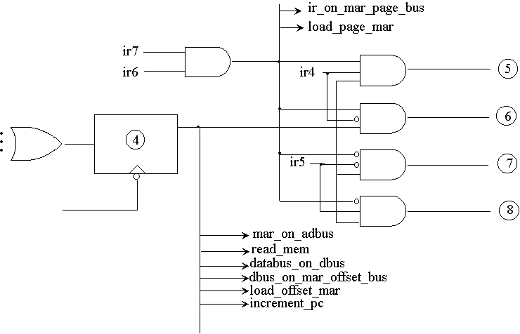
FIGURE 10. 58
State 4: completing address of full address instructions; branching for indirect, direct, jsr, and branch, (a) VHDL code, (b) Hardware.
s5: BLOCK (s(5) = '1')
BEGIN -- indirect addressing
-- read actual operand from memory into mar offset
mar_on_adbus <= GUARDED '1';
read_mem <= GUARDED '1' AFTER read_delay;
databus_on_dbus <= GUARDED '1';
dbus_on_mar_offset_bus <= GUARDED '1';
load_offset_mar <= GUARDED '1';
-- goto 6
ck: BLOCK ( (clk = '0' AND NOT clk'STABLE) AND GUARD )
BEGIN
s(6) <= GUARDED '1';
END BLOCK ck;
END BLOCK s5;

FIGURE 10. 59
State 5: taking care of indirect addressing.
BEGIN
jm : BLOCK ( (ir_lines (7 DOWNTO 5) = "100" ) AND GUARD
BEGIN
load_page_pc <= GUARDED '1';
load_offset_pc <= GUARDED '1';
-- goto 2
ck: BLOCK ( (clk = '0' AND NOT clk'STABLE) AND GUARD )
BEGIN
s(2) <= GUARDED '1';
END BLOCK ck;
END BLOCK jm;
st: BLOCK ( (ir_lines (7 DOWNTO 5) = "101") AND GUARD)
BEGIN
-- mar on adbus, ac on databus, write to memory
mar_on_adbus <= GUARDED '1';
alu_b <= GUARDED ‘1’;
obus_on_dbus <= GUARDED '1';
dbus_on_databus <= GUARDED '1';
write_mem <= GUARDED '1' AFTER write_delay;
-- goto 1
ck: BLOCK ( (clk = '0' AND NOT clk'STABLE) AND GUARD )
BEGIN
s(1) <= GUARDED '1';
END BLOCK ck;
END BLOCK st;
rd: BLOCK ( (ir_lines (7) = '0') AND GUARD)
BEGIN
-- mar on adbus, read memory for operand, perform operation
mar_on_adbus <= GUARDED '1';
read_mem <= GUARDED '1' AFTER read_delay;
databus_on_dbus <= GUARDED '1';
alu_a <= GUARDED ‘1’ WHEN ir_lines (6 DOWNTO 5) = "00" ELSE ‘0’;
alu_and <= GUARDED ‘1’ WHEN ir_lines (6 DOWNTO 5) = "01" ELSE ‘0’;
alu_add <= GUARDED ‘1’ WHEN ir_lines (6 DOWNTO 5) = "10" ELSE ‘0’;
alu_sub <= GUARDED ‘1’ WHEN ir_lines (6 DOWNTO 5) = "11" ELSE ‘0’;
load_sr <= GUARDED '1';
load_ac <= GUARDED '1';
-- goto 1
ck: BLOCK ( (clk = '0' AND NOT clk'STABLE) AND GUARD )
BEGIN
s(1) <= GUARDED '1';
END BLOCK ck;
END BLOCK rd; -- perform lda, and, add, sub
END BLOCK s6;

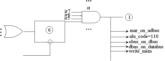
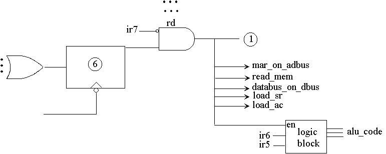
FIGURE 10. 60
State 6: reading the actual operand, and executing jmp, sta, lda, and, add, and sub instructions, (a) VHDL code, (b) Hardware.
s7: BLOCK (s(7) = '1')
BEGIN -- jsr
-- write pc offset to top of subroutine
mar_on_adbus <= GUARDED '1';
pc_offset_on_dbus <= GUARDED '1';
dbus_on_databus <= GUARDED '1';
write_mem <= GUARDED '1' AFTER write_delay;
-- address of subroutine to pc
load_offset_pc <= GUARDED '1';
-- goto 8
ck: BLOCK ( (clk = '0' AND NOT clk'STABLE) AND GUARD )
BEGIN
s(8) <= GUARDED '1';
END BLOCK ck;
END BLOCK s7;
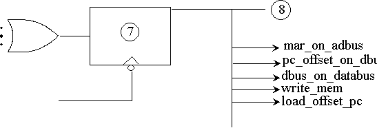
FIGURE 10. 61
State 7: writing return address of subroutine; making pc point to top of subroutine, (a) VHDL code, (b) Hardware.
s8: BLOCK (s(8) = '1')
BEGIN
-- increment pc
increment_pc <= GUARDED '1';
-- goto 1
ck: BLOCK ( (clk = '0' AND NOT clk'STABLE) AND GUARD )
BEGIN
s(1) <= GUARDED '1';
END BLOCK ck;
END BLOCK s8;

FIGURE 10. 62
State 8: incrementing pc to skip location reserved for return address, (a) VHDL code, (b) Hardware.
s9: BLOCK (s(9) = '1')
BEGIN
load_offset_pc <= GUARDED
'1' WHEN (status AND ir_lines (3 DOWNTO 0)) /= "0000" ELSE '0';
-- goto 1
ck: BLOCK ( (clk = '0' AND NOT clk'STABLE) AND GUARD )
BEGIN
s(1) <= GUARDED '1';
END BLOCK ck;
END BLOCK s9;
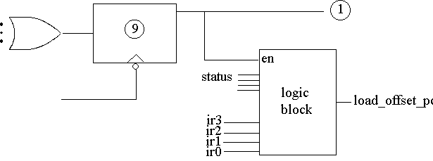
FIGURE 10. 63
State 9: conditional loading of pc for branch instructions, (a) VHDL code, (b) Hardware.
ck: BLOCK ( clk = '0' AND NOT clk'STABLE )
BEGIN
s (9 DOWNTO 1) <= GUARDED "000000000";
END BLOCK ck;
-- State blocks end here
END dataflow;
FIGURE 10. 64
A zero driver is placed on all state, ending the dataflow description of the par_control_unit.

FIGURE 10. 65
General outline of Parwan controller.
ENTITY par_central_processing_unit IS
PORT (clk : IN qit;
interrupt : IN qit;
read_mem, write_mem : OUT qit;
databus : INOUT wired_byte BUS := "ZZZZZZZZ"; adbus : OUT twelve
);
END par_central_processing_unit;
FIGURE 10. 66
Entity declaration of the Parwan CPU for its dataflow description.
ARCHITECTURE dataflow OF par_central_processing_unit IS
COMPONENT par_data_path
PORT (databus : INOUT wired_byte; adbus : OUT twelve;
clk : IN qit;
load_ac, zero_ac,
. . .
ir_lines : OUT byte; status : OUT nibble
);
END COMPONENT;
FOR data: par_data_path USE ENTITY WORK.par_data_path (structural);
--
COMPONENT par_control_unit
PORT (clk : IN qit;
load_ac, zero_ac,
. . .
ir_lines : IN byte; status : IN nibble;
read_mem, write_mem : OUT qit; interrupt : IN qit
);
END COMPONENT;
FOR ctrl: par_control_unit USE ENTITY WORK.par_control_unit (dataflow);
--
SIGNAL load_ac, zero_ac,
. . .
SIGNAL ir_lines : byte;
SIGNAL status : nibble;
BEGIN
data: par_data_path PORT MAP
(databus, adbus,
clk,
load_ac, zero_ac,
. . .
ir_lines, status
);
ctrl: par_control_unit PORT MAP
(clk,
load_ac, zero_ac,
. . .
ir_lines, status,
read_mem, write_mem, interrupt
);
END dataflow;
FIGURE 10. 67
The general outline of dataflow architectture of Parwan CPU.
ARCHITECTURE input_output OF parwan_tester IS
COMPONENT parwan PORT (clk : IN qit; interrupt : IN qit;
read_mem, write_mem : OUT qit;
databus : INOUT wired_byte BUS; adbus : OUT twelve );
END COMPONENT;
SIGNAL clock, interrupt, read, write : qit;
SIGNAL data : wired_byte := "ZZZZZZZZ";
SIGNAL address : twelve;
TYPE byte_memory IS ARRAY ( INTEGER RANGE <> ) OF byte;
BEGIN
int : interrupt <= '1', '0' AFTER 4500 NS;
clk : clock <= NOT clock AFTER 1 US WHEN NOW <= 140 US ELSE clock;
cpu : parwan PORT MAP (clock, interrupt, read, write, data, address);
mem : PROCESS
VARIABLE memory : byte_memory ( 0 TO 63 ) :=
("00000000", "00011000", "10100000", "00011001", --lda 24, sta 25
"00100000", "00011010", "01000000", "00011011", --and 26, add 27
"11100010", "11101001", "01100000", "00011100", --cac, asr, sub 28
"00010000", "00011101", "11000000", "00100100", --lda i 29, jsr 36
"11101000", "11100000", "10000000", "00100000", --asl, nop, jmp 32
"00000000", "00000000", "00000000", "00000000",
"01011100", "00000000", "01110000", "00010010", --(24, 25, 26, 27)
"00001100", "00011111", "00000000", "01011010", --(28, 29, 30, 31)
"10000000", "00010010", "00000000", "00000000", --jmp 18
"00000000", "11100010", "10010000", "00100100", -- , cma, jmp i 36
OTHERS => (OTHERS => ‘0’));
VARIABLE ia : INTEGER;
BEGIN
WAIT ON read, write;
qit2int (address, ia);
IF read = '1' THEN
IF ia >= 64 THEN
data <= "ZZZZZZZZ";
ELSE
data <= wired_byte ( memory (ia) );
END IF;
WAIT UNTIL read = '0';
data <= "ZZZZZZZZ";
ELSIF write = '1' THEN
IF ia < 64 THEN
memory (ia) := byte ( data );
END IF;
WAIT UNTIL write = '0';
END IF;
END PROCESS mem;
END input_output;
FIGURE 10. 68
A simple test bench for Parwan behavioral and dataflow descriptions.
CONFIGURATION behavior OF parwan_tester IS
FOR input_output
FOR cpu : parwan
USE ENTITY behavioral.par_central_processing_unit(behavioral);
END FOR;
END FOR;
END behavior;
(a)
CONFIGURATION dataflow OF parwan_tester IS
FOR input_output
FOR cpu : parwan
USE ENTITY par_dataflow.par_central_processing_unit(dataflow);
END FOR;
END FOR;
END dataflow;
(b)
FIGURE 10. 69
Configuring input_output architecture of Parwan tester (a) for testing behavioral architecture of par_central_processing_unit, (b) for testing dataflow architecture of par_central_processing_unit.
WHEN instr_fetch => ---------------------------------------2
-- read memory into ir
read_mem <= '1';
IF grant = '1' THEN
mar_on_adbus <= '1';
IF ready = '1' THEN
databus_on_dbus <= '1';
alu_a <= ‘1’;
load_ir <= '1';
increment_pc <= '1';
next_state <= do_one_bytes;
ELSE
next_state <= instr_fetch;
END IF;
ELSE
next_state <= instr_fetch;
END IF;
WHEN do_one_bytes => --------------------------------------3
. . .
FIGURE 10. 70
Memory and bus signaling for fetch state of controller.