

FIGURE 1. 1
A digital system design process

FIGURE 1. 2
Result of the data path design phase.
mark1 :=
BEGIN
** memory.state **
m[0:8191]<31:0>,
** processor.state **
pi\present.instruction<15:0>'
f\function<0:2> := pi<15:13>,
s<0:12> := pi<12:0>,
cr\control.register<12:0>,
acc\accumulator<31:0>,
** instruction.execution ** {tc}
MAIN i.cycle :=
BEGIN
pi = m[cr]<15:0> NEXT
DECODE f =>
BEGIN
0\jmp := cr = m[s],
1\jrp := cr = cr + m[s],
2\ldn := acc = - m[s],
3\sto := m[s] = acc,
4:5\sub := acc = acc - m[s],
6\cmp := IF acc LSS 0 => cr = cr + 1,
7\stp := STOP(),
END NEXT
cr = cr + 1 NEXT
RESTART i.cycle
END
FIGURE 1. 3
An ISPS example, a simple processor.
(Source: M. R. Barbacci, The ISPS Computer Description Language, Carnegie-Mellon University, 1981, p. 70.)
AHPLMODULE: multiplier.
MEMORY: ac1[4]; ac2[4]; count[2]; extra[4]; busy.
EXINPUTS: dataready.
EXBUSES: inputbus[8].
OUTPUTS: result[8]; done.
CLUNITS: INC[2](count); ADD[5](extra; ac2);
1 ac1 <= inputbus[0:5]; ac2 <= inputbus[4:7];
extra <= 4$0;
=> ( ^dataready, dataready ) / (1, 2).
2 busy <= \1\;
=> ( ^ac1[3], ac1[3] ) / (4, 3).
3 extra <= ADD[1:4] (extra; ac2).
4 extra, ac1 <= \0\, extra, ac1[0:2];
count <= INC(count);
=> ( ^(&/count), (&/count) ) / (2, 5).
5 result = extra, ac1; done = \1\; busy <= \0\;
=> (1).
ENDSEQUENCE
CONTROLRESET(1).
END.
FIGURE 1. 4
An AHPL example, showing a sequential multiplier.
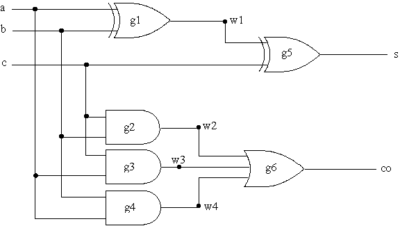
(a)
`timescale 1 ns / 1 ns
// A 6-gate full adder; this is a comment
module fulladder (s, co, a, b, c);
// Port declarations
output s, co;
input a, b, c;
// Intermediate wires
wire w1, w2, w3, w4;
// Netlist description
xor #(16, 12) g1 (w1, a, b);
xor #(16, 12) g5 (s, w1, c);
and #(12, 10) g2 (w2, c, b);
and #(12, 10) g3 (w3, c, a);
and #(12, 10) g4 (w4, b, a);
or #(12, 10) g6 (co, w2, w3, w4);
endmodule
(b)
FIGURE 1. 5
A full-adder, (a) logical diagram, (b) Verilog description.

FIGURE 1. 6
Hardware simulation.
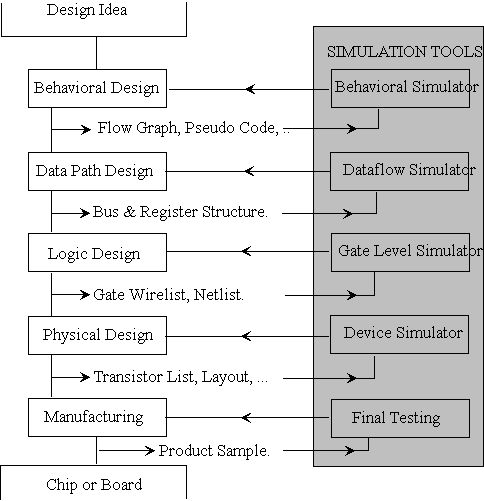
FIGURE 1. 7
Verifying each design stage by simulating its output.

(a)

(b)
FIGURE 1. 8
An exclusive-OR function in terms of AND, OR and NOT gates, (a) logical diagram, (b) test data.
|
GATE |
FUNCTION |
INPUT 1 |
INPUT 2 |
VALUE |
|
1 |
Input |
a |
-- |
0 |
|
2 |
Input |
b |
-- |
0 |
|
3 |
NOT |
2 |
-- |
1 |
|
4 |
NOT |
1 |
-- |
1 |
|
5 |
AND |
1 |
3 |
0 |
|
6 |
AND |
4 |
2 |
0 |
|
7 |
OR |
5 |
6 |
0 |
FIGURE 1. 9
Tabular representation of exclusive-OR circuit for oblivious simulation.
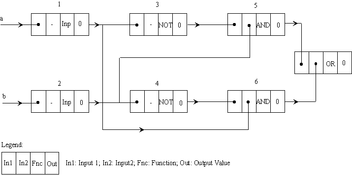
FIGURE 1. 10
Linked list representation of exclusive-OR circuit for event driven simulation.
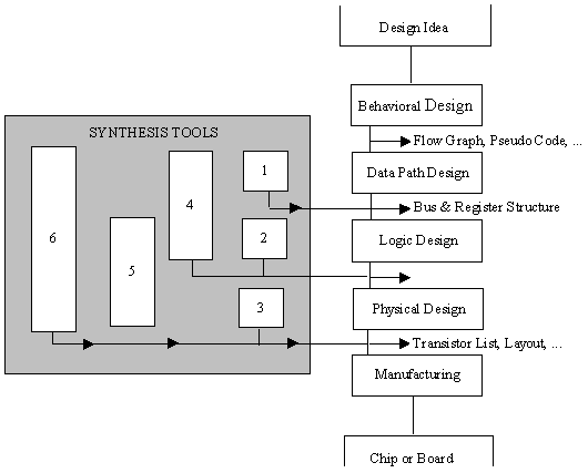
FIGURE 1. 11
Categories of synthesis tools in a design process.
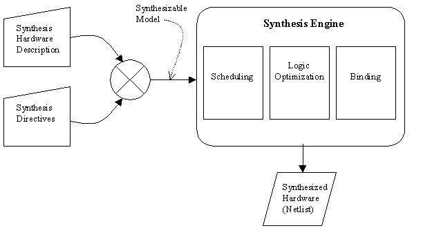
FIGURE 1. 12
Synthesis process.
 FIGURE 1. 13
Resource sharing.