| Lab2: Saturating Adder via VHDL | ||
| TOC
|
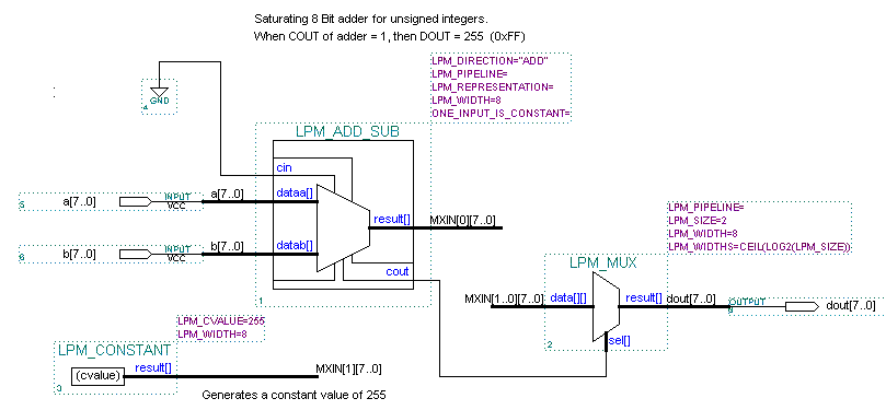
Objective:The objective of this lab is to introduce the student to a combinational logic block created via VHDL. To Do (part 1):A. The schematic below implements an 8-bit saturating adder for unsigned integers. If the carry out of the adder block is '1' indicating unsigned overflow, then the output will be clamped to 255 (0xFF). Saturating arithmetic is a common feature in 3D graphics and digital signal processing applications. You are to implement this functionality via one VHDL entity. You must use the same
external port names as shown on the schematic. SATADD schematic
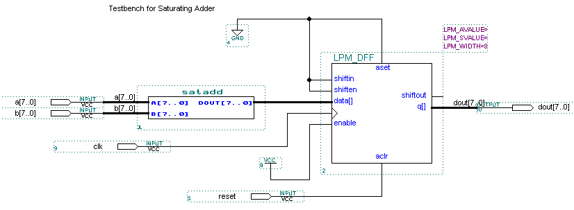
Testing Your Design TOCThe schematic below (TBSAT) is to be used to test your design. This testbench hooks up an 8-bit wide DFF to the output of satadd in order to register the output. The waveform file TBSAT.SCF can be used to test the design. The waveform file SATGOLD.SCF is the 'golden' file (correct expected results) that can be used to check your results. Use the FILE -> COMPARE command in the waveform editor to compare your TBSAT.SCF waveform against the SATGOLD.SCF waveform. RIGHT CLICK on each filename to save to disk: TBSAT.GDF, TBSAT.SCF, SATGOLD.SCF .
TO DO (part 2) TOCAfter verifying that your satadd design works correctly inside of the testbench, map your satadd design to both the EPF10K20RC240-2 and EPM7128SLC84-7 devices. Using the RPT file, give the total number of logic cells used in each technology. Use the timing analyzer and report the longest path from input to output for each implementation technology. To Turn InA printout of your VHDL file, and the information requested in Part 2. Check Off TOCYou must DEMONSTRATE you satadd design to the TA; you must demonstate that the waveforms produced using your satadd design within the testbench matches the golden result.
|
|

