| Lab3: Introduction to Altera LPMs | ||
| TOC
Multi-dimensional busses in Maxplus
|
Objective:The objective of this lab is to introduce the student to parameterized modules in Altera, particularly the mux and multiplier modules. To Do (part 1):The Altera parameterized modules offer a powerful method for building datapaths. Use the LPM_MUX, LPM_MULT modules to implement the following operation: Y = A * F where A is an 8 bit number representing a fixed point number 0.xxxxxxxx that will range from 0.0 to 0.996 . All possible 8-bit codes are valid for input A. The input F is a 9 bit number that will range from 0 to 1.0 . In binary, this range will be 000000000 to 100000000 (note that there are 9 binary digits). Not all possible 9-bit codes are valid for F; the only valid input for F in which the most significant bit is a '1' is the code 100000000 which represents the decimal value 1.0 . The multiplication should use all 8 bits of A and only the lower 8 bits of F. If the most significant bit of F is a '1' indicating that the F input is a 1.0, then the output of the multiplier should be ignored and the Y output should be equal to A. (1.0 * A = A). The reason that the multiplier output should be ignored in this case is because the multiplier output will be 0 since the lower 8 bits of F will be all zeros. You are to implement this function using the LPM_MULT and LPM_MUX parameterized modules. If you find that you need other functionality, then you may use either VHDL or schematic capture to implement the functionality. Your design should be named fmult. LPM_MULT TOCThe parameterized module LPM_MULT is used to implement the multiplication operation. Performing a K x M bit binary multiplication will result in a product that is K+M bits wide. If both operands are the same width (N x N), then the product will be 2N bits wide. If the input numbers represent fractional quantities (i.e, fixed point numbers between 0.0 =< x < 1.0), then it is common practice to drop the lower N bits from the 2N bit product in order to keep the product the same width as the operands (dropping the lower N bits drops the N least significant bits, so the final result is close to the correct result). The parameters for the LPM_MULT module should be set as follows:
The other parameters can be left to their defaults. When you compile your design, you will get a warning about the least significant bits of the product being discarded -- this is ok. LPM_MUXThe LPM_MUX parameterized mux is straightforward. The parameters control the width of the inputs (LPM_WIDTH) and the number of inputs (LPM_SIZE) Multi-dimensional busses in Maxplus TOCThe parameterized modules make extensive use of multi-dimensional busses. A multi-dimensional bus can be thought of as a group of busses which are all the same width. Suppose I need two 8-bit busses. I could declare two separate busses:
or one multi-dimensional bus:
I could refer to each of the 8-bit busses in the multi-dimensional bus via the names:
In the LPM_MUX module, if you set LPM_WIDTH=8, LPM_SIZE=4 (4 inputs, each 8 bits wide), you will get a symbol whose input bus needs to be labeled as:
Connecting Single Dimensional Busses to Multi-Dimensional BussesYou may often find it necessary to connect a single dimensional bus to a multi-dimensional bus:
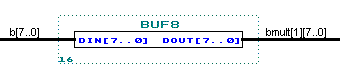
The only way I have been able to do this is by using buffers to connect the two busses. For convenience purposes, I created a VHDL file called buf8 that I use for connecting an 8-bit 1D bus to an 8-bit 2D bus. Example usage of this is shown below:
The VHDL for BUF8 can be found here.
Testing Your Design TOCThe TBMULT.GDF file below is a testbench that you can use to test your design. The TBMULT.SCF file is input waveform file; the TBMULTGOLD.SCF is the golden waveform (compare this against the waveform that you get). RIGHT CLICK on each filename to save to disk: TBMULT.GDF, TBMULT.SCF, TBMULTGOLD.SCF .
TO DO (part 2) TOCSynthesis Options (NORMAL)After verifying that your fmult design works correctly inside of the testbench, map your fmult design tothe EPF10K20RC240-2 (Flex 10K) device. When doing the synthesis, use the "Assign -> Global Project Logic Synthesis" and ensure that the the synthesis style is NORMAL. Make sure the Area/Speed tradeoff slider is set at 5. Use the "Define Synthesis Style" button and ensure that the "Carry Chain" and "Cascade Chain" options are set to "Ignore". Using the RPT file, give the total number of logic cells used in each technology. Use the timing analyzer and report the longest path from input to output. Also, use the floorplan editor (Menu "MaxPlusII -> FloorPlan Editor") to visually inspect how much of the chip contains logic. Synthesis Options (FAST)Using the same device as above, change the synthesis style to FAST using the "Assign-> Global Project Logic Synthesis". Make sure that the Area/Speed tradeoff slider is set at 10. Use the "Define Synthesis Style" button amd ensure that the "Carry Chain" and "Cacade Chain" options are set to "Auto". Using the RPT file, give the total number of logic cells used in each technology. Use the timing analyzer and report the longest path from input to output. Also, use the floorplan editor (Menu "MaxPlusII -> FloorPlan Editor") to visually inspect how much of the chip contains logic. Report if any Cascade or Carry Chains are used (should be visible in the floorplan). Compare both the maximum propagation times and # of logic cells generated via the NORMAL and FAST synthesis options. To Turn InA plot of your schematic, and the information requested in Part 2. Check Off TOCYou must DEMONSTRATE you fmult design to the TA; you must demonstrate that the waveforms produced using your fmult design within the testbench matches the golden result.
|
|