VHDL Interfaces and Example
Designs for the XSV board 1.0

Introduction and Overview
Project Supervisor - Peter Sutton
4.0
Development platform and tools 3
5.0
Design flow for FPGA designs
5.4
Configuring the Virtex FPGA
6.0
Design flow for CPLD designs
1.0 About these resources
“VHDL Interfaces and Example Designs for the XSV Board 1.0” is a
collection of resources to be used with the XSV board v1.0, produced by XESS
Corp. This board contains a Virtex FPGA from Xilinx Inc. and support circuitry
for communicating with a wide variety of external devices. This set of resources
is designed to provide a set of VHDL entities that act as interfaces to the
various capabilities and devices on the XSV board, as well as sample designs
that demonstrate the use of the board’s main features. The resources were
developed internally by students at the
Most of these resources consist of VHDL source code and the accompanying
documentation. For a list of the resources, see section 3.0, “List of designs”.
2.0 About this document
This Introduction and Overview serves as a summary of all the resources
in this collection. It lists all the resources in the collection and provides information
that is common to most of the designs. For example, the basic design flow used
to synthesize and implement the VHDL source code is explained in this document.
3.0 List of designs
Most of resources in this collection can be grouped into the following
two categories:
3.1 VHDL modules
These consist of VHDL entities that act as interfaces to the peripheral
capabilities of the XSV board. These entities are designed to be embedded in a
larger, arbitrary design, which will often be referred to as the “user” design.
The VHDL modules are designed to make it easier for a user design to interact
with the various external devices that can be attached to the XSV board (e.g.
audio in/out, video in/out, Ethernet network connection).
Most VHDL modules also come with an accompanying stand-alone design that
demonstrates the use of the module. The VHDL modules cannot be directly
implemented on the Virtex FPGA without an accompanying top-level entity.
3.2 Stand-alone VHDL designs
These sets of VHDL source files always include a top-level entity. As
such, stand-alone designs can be directly implemented on the Virtex FPGA and do
not need to be incorporated in a larger user design. Stand-alone designs serve
as examples of how to use the peripheral capabilities of the board. Many of the
stand-alone designs include modules that can be used separately in a user’s own
design.
Each stand-alone design comes with a UCF file that ensures it will be
correctly implemented on the XSV board. Most of the constraints in these files
are pin constraints.
3.3 Other designs
As well as modules and stand-alone designs, there is also a Visual Basic
programme that accompanies one of the modules to provide communication between
the XSV board and a PC.
3.4 List of designs
|
Design Name |
Type |
Explanation |
|
VHDL IP Stack |
Modules and
stand-alone. |
Uses the Ethernet
PHY chip on the XSV board. Provides an implementation of Ethernet, IP and
several transport protocols. |
|
Audio Project |
Modules and stand-alone. |
Uses the stereo
codec chip on the XSV board. Records data from the audio port and stores it
in SRAM. Allows the recorded audio to be played back again. |
|
VGA Interface |
Modules and
stand-alone. |
Uses the RAMDAC and
VGA monitor interface on the XSV board. Displays test patterns on a VGA
monitor, using several different D/A conversion modes. |
|
Video Input
Project |
Stand-alone only. |
Uses the video
decoder chip on the XSV board. Decodes RCA and S-Video signals into pixel
data, which is stored in SRAM. This data is then sent to a VGA monitor. |
|
SRAM Interface |
Modules only. |
Uses the two
banks of SRAM provided on the XSV board. Provides a simpler synchronous
interface to either bank of SRAM. |
|
PC to SRAM Interface |
Modules and
stand-alone. |
Uses the parallel
port connections on the XSV board. Uses VHDL modules to allow a PC programme
to read and write to any location of the XSV board’s SRAM through the
parallel port. A Visual Basic utility programme that utilises these
capabilities is also provided. |
|
CPLD SVF File
Descriptions |
Stand-alone only. |
A number of
designs for the CPLD on the XSV board are provided. Most of these make only
minor changes to the default design for the CPLD provided by XESS. |
|
PS/2
Encoder/Decoder |
Stand-alone only. |
Uses the PS2
connections on the XSV board. Displays data received from a PS2 device and
can send data to a PS2 device. |
4.0 Development platform and tools
These resources have been developed using the following platforms and
tools:
|
Item: |
Details: |
Company: |
|
FPGA development
board |
XSV-300 v1.0 ·
Includes
a Virtex xcv300-4-pq240 (300 000 gates, speed grade 4) from Xilinx Inc. ·
A standard
ATX power supply was used. |
XESS Corp. |
|
PC Platform |
Windows 98 (PII,
350MHz, 128 MB RAM) |
Microsoft Corp. |
|
Board
configuration software |
XSVTOOLs v3.2 ·
Virtex
configuration was performed using the GXSLOAD tool using the parallel port. |
XESS Corp. |
|
VHDL design
environment |
Foundation F3.1i |
Xilinx Inc. |
|
PC software
development |
Microsoft Visual
Basic v6.0 (as part of Microsoft Visual Studio) |
Microsoft Corp. |
5.0 Design flow for FPGA designs
This section explains the basic design flow used to synthesise and
implement a VHDL stand-alone design for the Virtex FPGA. It is assumed that the
reader is using the same development tools listed in section 4.0 of this
document, but particularly that they are using Xilinx Foundation F3.1i and
XSVTOOLs v3.2. It is assumed that these tools have been successfully installed.
The design flow described should apply to all the VHDL designs in this
collection for the FPGA. As an example, the design flow will be explained step
by step for the Audio Project design.
5.1 Creating the project
1.
Create a folder to contain the project description
file (*.pdf file) and all the project’s associated files.
Example: The example in this
section will explain the design flow for the Audio Project design. To begin
with, we create a folder on C:\ called “audio”.
2.
Start the Foundation Project Manager by clicking:
Start / Programs / Xilinx Foundation Series 3.1i / Project Manager.
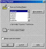
3.
In the “Getting Started” dialog box, select “Create a
New Project” and click OK.
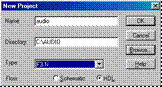
4.
In the “Name” field, type a name for your project.
Change the “Directory” field to the folder you created in step 1. (Clicking
“Browse” lets you find the folder graphically). The value for “Type” should read
“F3.1i” (the same as the version of Foundation). For the “Flow” heading, select
the “HDL” option. Then press OK.
Example: We will call the
project “audio” to match our directory name. The completed dialog box for this
example should look like the following:
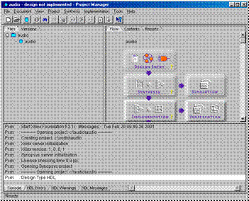
Foundation will
create a folder with the pathname “C:\audio\audio”. The Project Manager window
should now look something like the following:
5.
You now need to add the VHDL files to the project.
Click on the “Project” menu and select “Add Source File(s)…”. A standard “Open”
dialog box will be displayed. Select the file you wish to add to the project,
then click “Open”. You can hold down the Shift or Ctrl keys to select multiple
files within the dialog box.
Example: The Audio Project
design consists of the following files:
·
audio.vhd
·
audiotop.vhd
·
player.vhd
·
recorder.vhd
·
remap.vhd
·
sram512k32bit50mhz-sv05.vhd
After saving these files to
your local hard drive, add each of them to the “audio” project using the
procedure described above. After doing this, the Project Manager window should look
something like the following:
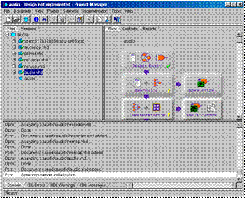
As each VHDL file is added to the project,
Foundation will analyse the syntax of each file. It will report any errors it
finds in the console section of the main window.
To edit any of the VHDL files in the project,
simply double-click on the name of the file in the Project Manager window. This
will open the HDL editor. When you open the editor in this way, any changes you
save are automatically detected by the Project Manager.
If at some stage you make changes to a source
file but the Project Manager does not detect that your file has changed, you
can force it to notice the changes by telling it to re-analyse the file. To do
this, right-click on the file in the Project Manager and select “Force
Analysis”. To do this for every file in the project, click the “Synthesis” menu
and select “Force Analysis of All Sources”.
5.2 Synthesizing the project
6.
Once all the VHDL source files have been added to the
project, you can synthesize the design. In order to perform synthesis for the
first time, Foundation needs to know which of your VHDL entities is the
top-level entity. Conversely, when you specify the top-level entity, Foundation
automatically assumes that you wish to synthesize your design.
So,
to specify the top-level entity and synthesize the design, click on the
plus-sign next to the file containing the top-level entity. A list of the VHDL
entities contained in that file is displayed. Right-click on the entity that is
to be the top-level entity and select “Set as Top Level…”.
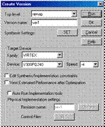
The
“Create Version” dialog box is displayed.
Example: In the Audio Project
design, the file “remap.vhd” contains the top-level entity, also called
“remap”. Carry out the instructions above to set “remap” as the top-level
entity.
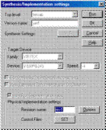
7.
In the “Create
Version” dialog box, ensure that the target device matches the Virtex FPGA on
your XSV board. The “Family” heading should read “Virtex”. The “Device” and
“Speed” headings can be determined from the markings on your FPGA. Do not press
“Run” nor “OK” just yet.
Example: Our FPGA has the
following markings, which determine the values to be set in this dialog box:
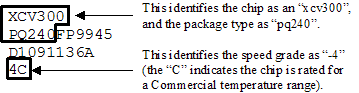
We therefore set
“Device” to “V300PQ240” and “Speed” to “-4”. The dialog box should look
something like the following:
8.
Foundation allows you to set some options that control
synthesis. To set these click the “SET” button to the right of the “Synthesis
Settings” heading. The following dialog box will be displayed:
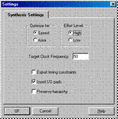
Set any of these options that you wish to, then
click OK.
Example: The Audio Project
project is designed to work with a 50MHz clock signal. We specify this by
entering “50” under the “Target Clock Frequency” heading. This setting does not
guarantee that a particular design will work at the specified frequency, but it
provides the synthesis engine with a target frequency to aim for.
We also choose
to optimise for “Speed” and set the synthesis effort level to “High”. We then
click OK.
To commence synthesis, click “Run” in the
“Create Version” dialog box.
Foundation will synthesize the design,
reporting the results in the “Console” section of the main window.
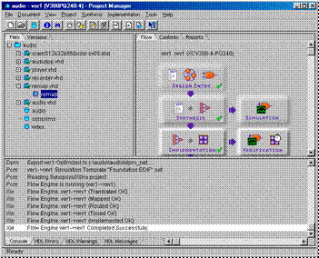
Example: If synthesis is
successful, the main window should look something like the following:
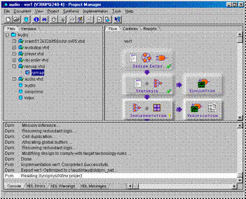
Any errors that occur during synthesis will
also be reported in the “Console” section of the window.
Note that Foundation attaches its own version
number to every successful synthesis of a project. This version number is shown
in the “Flow” section of the main window.
At this stage of the design flow, you can
simulate the synthesised design by clicking on the “Simulation” button. This
launches the Logic Simulator which allows you to simulate and test the design
using a graphical interface.
The Implementation phase of the design flow can
now be run.
5.3 Implementing the project
9.
Click on the “Implementation” button in the “Flow”
section of the main window. The “Synthesis/Implementation settings” dialog box
is displayed, as shown below. This is identical to the “Create Version” dialog
box displayed previously, but now only the options relating to Implementation
are available to be modified.
Clicking the “Options” button displays the
following dialog box, which allows various options for different steps of the
Implementation design flow to be adjusted:
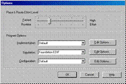
The main option you may wish to adjust is the
Place & Route Effort Level. Click OK to return to the
“Synthesis/Implementation settings” dialog box.
Example: For the Audio Project
design, you can leave all the options at their default values. This means you
don’t need to change the Place & Route Effort Level.
10.
All stand-alone designs in this collection have an
associated User Constraints File (UCF) that specifies which ports in the VHDL
design are connected to which pins on the Virtex FPGA.
The “Synthesis/Implementation settings” dialog
box should still be visible. To specify a UCF to the Implementation tools,
click the “SET” button to the right of
the “Control Files” heading. The following “Settings” dialog box is
displayed:
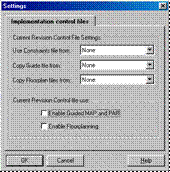
11.
Click the down arrow next to the “Use Constraints file
from” and click “Custom”. A dialog box appears allowing you to specify the UCF.
Clicking “Browse” allows you to select the UCF graphically.
Example: The UCF for the Audio
Project is called “audiopins.ucf”.
Specify this file in the “Custom” dialog box and click “OK”.
Click “OK” in the “Settings” dialog box.
Finally, click “Run” to commence the
Implementation design flow.
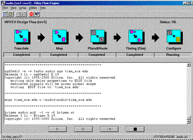
The Foundation Flow Engine will commence. The
report files from each stage of the implementation are shown in the log section
of Flow Engine window as the implementation progresses, as shown below:
Example: When the
Implementation has successfully completed, the main Project Manager window should
look something like the following:
Note that Foundation attaches its own revision
number to every successful implementation of a project. This revision number is
shown alongside the version number in the “Flow” section of the main window.
12.
Before configuring the Virtex FPGA with the new
implementation, it is wise to confirm that the pin constraints from the UCF
were adhered to. To do this, click on the Tools menu and select Implementation
/ Constraints Editor.
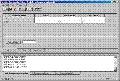
The Xilinx Constraints Editor will open, as
shown below:
13.
To confirm that the pin constraints have been adhered
to, click on the “Ports” tab (about halfway down the window on the left). The
Constraints Editor will show a list of all the ports for the design. If the pin
constraints have been adhered to, the column headed “Location” should be full
of pin numbers, as shown below. There should be one pin number for every port.
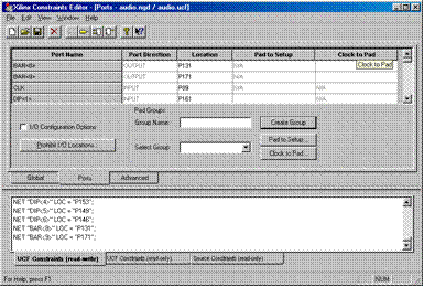
If the column headed “Location” is blank, you
need to respecify the UCF and re-implement the design. To do this:
·
Close the Constraints Editor.
·
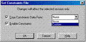
In the Program Manager, click the Implementation menu
and select “Set Constraints File(s)…”. This will show the “Set Constraints
File” dialog box.
·
In this dialog box, check the “Copy Constraints Data
From” option and select “Custom” from the drop down menu, as shown below:
·
·
A dialog box appears allowing you to specify the UCF.
Clicking “Browse” allows you to select the UCF graphically.
·
Once you have specified the UCF, click “OK” in the
“Set Constraints File” dialog box.
·
Click the “Implementation” button again. A dialog box
will appear asking if you wish to start the Implementation flow from the
“Translate” step again (shown below).
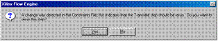
·
Click “Yes”. The Implementation flow will be re-run.
The Configuration stage of the implementation
(the last stage in the flow), generated a bit file (*.bit) that is downloaded
to the Virtex FPGA to configure it to the current design. This downloading and
configuration process can now be carried out.
5.4 Configuring the Virtex FPGA
14.
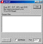
Open the GXSLOAD programme (part of the XSVTOOLs suite
of programmes from XESS Corp.). This displays the GXSLOAD window, as shown
below:
15.
Open the folder that was created for the project in
step 1. Open the folder whose name is the same as the name of the project. Open
the folder called “xproj”. Open the folder corresponding to the current version
of the project. Finally, open the folder corresponding to the current revision
of the project. (The version and revision numbers referred to here refer to
those displayed by Foundation in the main window of the Project Manager).
Locate the file in this folder with the same
name as the project and the file extension “.bit”. This is the bit file that
will be downloaded to the Virtex FPGA.
Example: For our example, we
open the folders outlined above, to reach the following location:
“C:\audio\audio\xproj\ver1\rev1\”
The bit file we
need in this folder is called “audio.bit”
16.
Ensure that the XSV board is powered on and that it is
connected to the computer via the parallel cable. In GXSLOAD, select the
parallel port being used (next to the “Port” heading).
17.
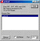
Drag the bit file from the folder in which it is
located, into the section of the GXSLOAD window headed “Recent Files”. GXSLOAD
will download the bit file to the Virtex FPGA, thus configuring it with the
current design.
Example: When the bit file for
the Audio Project has successfully been downloaded, GXSLOAD should look
something like the following:
That’s it. The Virtex FPGA should now be correctly
configured with the design described by the VHDL project.
6.0 Design flow for CPLD designs
Some of the designs for the Virtex FPGA also
require the CPLD on the XSV board to be reprogrammed. Reprogramming the CPLD
should be done cautiously, as if programming is not done correctly there is
potential for the CPLD to become completely unusable. See http://www.xess.com/appnotes/an-041000-xsvpport.pdf
for more information.
This section explains the design flow for a
VHDL design for the CPLD on the XSV board. Before reading this section you
should be familiar with section 5.0, “Design flow for FPGA designs”. It is
assumed that the reader is using the same development tools listed in section
4.0 of this document, but particularly that they are using Xilinx Foundation
F3.1i and XSVTOOLs v3.2. It is assumed that these tools have been successfully
installed. The design flow described should apply to all the VHDL files in this
collection containing designs for the CPLD. As an example, the design flow will
be explained step by step for the CPLD design that accompanies the IP Stack
design for the FPGA.
6.1 Creating the project
1.
to 5. Follow steps 1 to 5 for the FPGA design
flow, but instead creating a project for the CPLD design.
Example: The example in this
section will explain the design flow for the CPLD design that accompanies the
IP Stack design for the FPGA. We create a folder for the project with the path
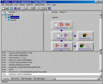
“C:\cpldnet” and create a project with the name “cpldnet”.
The design
contains a single VHDL file, called “cpldnet.vhd”, which we add to the project.
The resulting Project Manager window should look like this:
6.2 Synthesizing the project
6.
Click on the “Synthesis” menu and select “Options”.
The “Synthesis Options” dialog box will appear. Under the heading “FSM
Synthesis: Default Encoding”, choose the “Binary” option, as shown below. As a
general rule, a CPLD has fewer flip-flops than an FPGA. Selecting a binary
encoding of states (for a state machine) will result in fewer flip-flops being
used by any state machines in the design.
Click “OK” to close the “Synthesis Options”
dialog box.
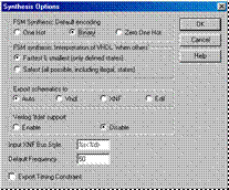
Foundation will then ask you to re-analyse all
the source files in order for the synthesis options to take effect.
7.
Click the “Synthesis” menu and select “Force Analysis
of All Sources”.
8.
The top-level entity of the design must now be
specified in order for synthesis to be performed correctly. Click on the plus-sign
next to the file containing the top-level entity. A list of the VHDL entities
contained in that file is displayed. Right-click on the entity that is to be
the top-level entity and select “Set as Top Level…”.
The
“Create Version” dialog box is displayed.
Example: The CPLD design for
the IP Stack PGA design has only one file, “cpldnet.vhd”. This contains a
single entity called “dwnldpar”, which is the top-level entity. Follow the
above instructions to specify “dwnldpar” as the top-level entity.
9.
In the “Create Version” dialog box, ensure that the
target device matches the CPLD on your XSV board. The “Family” heading should
read “XC9500”. The “Device” and “Speed” headings can be determined from the
markings on the CPLD. Do not press “Run” nor “OK” just yet.
Example: Our CPLD has the
following markings, which determine the values to be set in this dialog box:
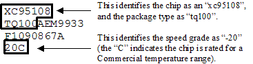
We therefore set
“Device” to “95108TQ100” and “Speed” to “-20”. The dialog box should look
something like the following:
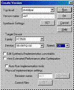
10.
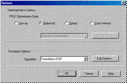
If it is necessary to set synthesis options, click the
“SET” button to the right of the “Synthesis Settings” heading.
Example: For our CPLD example
it is not necessary to change any synthesis options. The default values are
correct.
To commence synthesis, click “Run” in the “Create
Version” dialog box.
Foundation will synthesise the design,
reporting the results in the “Console” section of the main window.
6.3 Implementing the project
11.
Click on the “Implementation” button. The
“Synthesis/Implementation settings” dialog box is displayed, as shown below.
This is identical to the “Create Version” dialog box displayed previously, but
now only the options relating to Implementation are available to be modified.
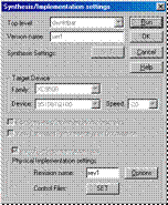
Clicking the “Options” button displays the
following dialog box, which allows various options for different steps of the
Implementation design flow to be adjusted:
Example: For this CPLD project,
you can leave all the implementation options at their default values.
Click “OK” to return to the “Synthesis/Implementation
settings” dialog box.
12.
A CPLD design will also usually have a User
Constraints File (UCF) which at the very least will specify which ports in the
VHDL design are connected to which pins on the CPLD.
The “Synthesis/Implementation settings” dialog
box should still be visible. To specify a UCF to the Implementation tools,
click the “SET” button to the right of
the “Control Files” heading. The following “Settings” dialog box is
displayed:
13.
Click the down arrow next to the “Use Constraints file
from” heading and click “Custom”. A dialog box appears allowing you to specify
the UCF. Clicking “Browse” allows you to select the UCF graphically.
Example: The UCF for this CPLD
project is called “cpldnetpins.ucf”. Specify this file in the “Custom” dialog
box and click “OK”.
Click “OK” in the “Settings” dialog box.
Finally, click “Run” to commence the
Implementation design flow.
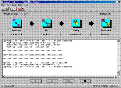
The Foundation Flow Engine will commence. The
report files from each stage of the implementation are shown in the log section
of Flow Engine window as the implementation progresses, as shown below:
14.
Before configuring the CPLD with the new
implementation, we should double check the pin constraints.
Important: It especially important when implementing
a CPLD design to check that the pin constraints specified in the UCF have
indeed been put in place by the implementation tools. This can be
checked by using the Xilinx Constraints Editor, available from the Project
Manager by clicking the Tools menu and selecting Implementation / Constraints
Editor. (See steps 12 and 13 from section 5.3 for a more detailed description
of how to perform this check).
Carefully check that the only
pins that have been set to be outputs are those that you intend to be outputs.
In particular, be careful if you are setting any of the CPLD pins connected to
pins C1, C2, C3 or S7 of the parallel port as outputs. If you are, then ensure
that you follow the instructions found in the “
The CPLD is configured using a type of file
known as an SVF file (not a BIT file). This SVF file must now be
created.
6.4 Creating the SVF file
15.
In the “Flow” section of the main Project Manager
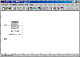
window, scroll down so that the “Programming” button is visible. Click the
“Programming” button. The Xilinx JTAG programmer should open, as shown below:
16.
Click on the “Output” menu and select “Create SVF
File…”. The “SVF Options” dialog box is displayed:
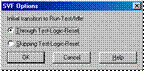
17.
Select the “Through Test-Logic-Reset” option and click
“OK”. The JTAG Programmer will prompt you for a filename and location for the
SVF. The default filename should be the name of the project with the extension
“.svf”. The default location should be in a hierarchy of folders based on the
project name, the current version number and the current revision number.
Click “Save” to accept the default filename and
location for the SVF file.
18.
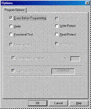
Click on the “Operations” menu and select “Program”.
The following “Options” dialog box will appear. Accept the default options and
click “OK”.
The JTAG programmer will then create the SVF
file. An “Operation Status” dialog box shows the progress of creating the SVF
file.
Example: When the SVF file has
been successfully completed, the “Operation Status” dialog should look
something like the following:
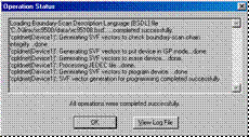
Click “OK” to close the “Operation Status” dialog
box. The SVF is now ready and can be downloaded to the CPLD to configure the
chip with the current design.
6.5 Configuring the CPLD
19.
Open the GXSLOAD programme (part of the XSVTOOLs suite
of programmes from XESS Corp.). Note that GXSLOAD can be used to download
multiple different file types to the XSV board, including BIT and (more
importantly here) SVF files as well.
20.
Open the folder containing the SVF file that has just
been created.
Example: For our example
(assuming that the SVF file was saved in the default location), the SVF file
will be found in the following folder:
“C:\cpldnet\cpldnet\xproj\ver1\rev1”
The SVF file we
need in this folder (assuming the SVF file was saved with the default filename)
is called “cpldnet.svf”.
21.
Ensure that the XSV board is powered on and that it is
connected to the computer via the parallel cable. In GXSLOAD, select the
parallel port being used (next to the “Port” heading).
22.
On the XSV board, ensure that a shunt is placed on
jumper J23. This shunt must be in place for the CPLD to be programmed. To
locate the position of jumper J23, see the board layout diagram in the XSV
board manual, available at http://www.xess.com/manuals/xsv-manual-1_0.pdf.
23.
Drag the SVF file from the folder in which it is
located, into the section of the GXSLOAD window headed “Recent Files”. GXSLOAD
will download the SVF file to the CPLD, thus configuring it with the current design.
24.
Remove the shunt from jumper J23 on the XSV board.
When this shunt is removed, it is impossible for the CPLD to be reprogrammed.
Removing this shunt therefore prevents accidental reprogramming of the CPLD.
That’s it. The CPLD should now be correctly
configured with the design described by the VHDL project.