System-on-a-Programmable-Chip Development Board
 1999년 9월경 Altera에서 발표했던 SOPC Board에 대해 정리를 하였습니다... 지금은 대부분의 사람들이 이 Board의 존재에 대해서 전혀 기억을 못하고 있는 추억의 물건입니다... (ALTERA USA의 기술지원 부서에다가 회로도 좀 구할 수 있냐고 했었는데요, 거기서도 없다고 할 정도니...) 1999년 9월경 Altera에서 발표했던 SOPC Board에 대해 정리를 하였습니다... 지금은 대부분의 사람들이 이 Board의 존재에 대해서 전혀 기억을 못하고 있는 추억의 물건입니다... (ALTERA USA의 기술지원 부서에다가 회로도 좀 구할 수 있냐고 했었는데요, 거기서도 없다고 할 정도니...)
최초 APEX 20K 시리즈가 발표된 후, 당시 최고급 제품이었던 APEX의 특징을 잘 나타낼 수 있는 방법의 하나로 이 SOPC Board가 선을 보였었고, 추후 APEX 20KE 시리즈가 나온 후에는 내장 Device를 EP20K1500E로 한 제품도 선을 보였었습니다...
제품의 주된 용도는 Board 명에서도 알 수 있듯이 ALTERA가 광고하던 System-on-a-Programmable-Chip Solution을 APEX20K 제품군으로 구현 및 Test해 보기위한 목적이었습니다... (제품에 포함된 문서에 보면, rapid prototyping, real-time emulation, system performance measurement등의 용도로 활용이 가능하다고 되어있습니다...)
어쨌거나, 지금은 "Excalibur EPXA10 DDR Development Kit"나 "NIOS Development Kit"등에게 그 자리를 물려주고, ALTERA Homepage에서도 정보가 사라져 버린 추억의 제품이 되어 버렸습니다...
SOPC Development Board Package 구성물
Board Feature
- Powerful development board for system-on-a-programmable-chip designs
- Features an APEX EP20K400 device
- Supports microprocessor intellectual property (IP)-based design
- Industry-standard interconnects
- 10/100 Ethernet with full and half duplexing
- Peripheral component interconnect (PCI) mezzanine connector
- High- and low-speed universal serial bus (USB) host supporting the Universal Serial Bus Specification, Revision 1.0
- IEEE Std. 1394A at 100, 200, and 400 Mbits/second
- IEEE Std. 1284 parallel interface
- 2 RS-232 ports (DCE and DTE)
- 2 PS/2 ports for mouse and keyboard
- Memory subsystem
- 2 banks of 1-Mbyte cache memory
- 64-Mbyte SDRAM in a DIMM socket
- 4-Mbyte FLASH memory
- 256-Kbyte EPROM
- Multiple clocks for communications systems design
- Multiple debug ports
- SignalTap embedded logic analyzer
- IEEE Std. 1149.1 Joint Test Action Group (JTAG)
- Extended JTAG (EJTAG)
- Supports 50 user I/O lines
- Additional features
- VGA monitor interface
- 4 user-defined switches and 6 LEDs
- Liquid crystal display
- Application LEDs
- Applications
- Embedded systems prototyping
- Communications systems design
- IP development and debugging
일반정보
The Altera system-on-a-programmable chip board is a development and prototyping platform that provides system designers with an economical solution to hardware verification. Unlike other development boards, the Altera system-on-a-programmable chip board supports a variety of microprocessor-based designs by incorporating memory, debugging, and interface resources.
The board is primarily designed for implementing microprocessor functions and other standard IP functions in the on-board APEX device. The board includes physical interfaces for widely used standard interconnects; control logic for the interconnects can be implemented in the device.
The board also supports EJTAG for development and debugging of MIPS-like microprocessor functions, as well as JTAG for other system testing. For additional analysis, the JTAG port can be used with the SignalTap embedded logic analyzer available with the Altera Quartus development software.
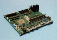
Board 사진

그림을 클릭하시면 고해상도 원본그림을 보실수 있습니다... [1,311 pixels X 919 pixels, (359,367 bytes)]
Related Links
|