Logic Synthesis with VHDL
Sequential Circuits
Bob Reese
Electrical Engineering Department
Mississippi State University
Converted to HTML by
MANJUNATH R. MITTHA
MS Student, Dept. of Elec. Eng.,
Mississippi State University
INDEX
Sequential Circuits
Sequential Template
8 bit Loadable Register with Asynchronous Clear
Reg8bit State Process
Wait Statement
Finite State Machine Example
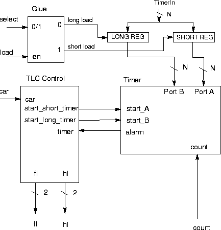
Traffic Light Controller Block Diagram
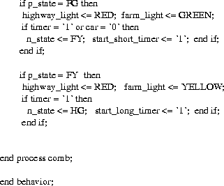
VHDL for TrafficLight FSM Control
One Hot Encoding for FSM's
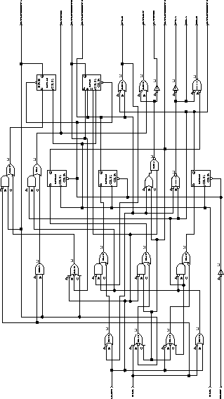
One Hot Encoding for TLC
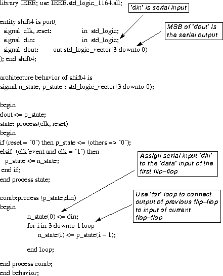
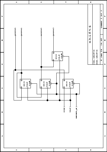
Simple 4 bit Shift Register
Loop Function for Shift Register
Scan Path Synthesis
4 Bit Register with Scan Path
Adding Scan to tlc_onehot.vhd
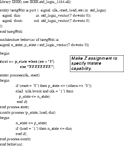
Register with Tri State Output
- Logic which contains both combinational logic and storage elements form sequential circuits.
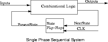
All sequential circuits can be divided into a combinational block and a storage element block.

- The above diagram shows a single*phase sequential system. In a single*phase system
the storage elements are edge-triggered devices (flip*flops).
- Moore-type outputs are a combinatorial function of PresentState signals.
- Moore-type outputs are a combinatorial function of both PresentState and external
input signals.
- Multiple*phase design is also supported since latches can be synthesized as the storage
elements.
BACK TO INDEX
library declarations

entity  model_name is
port
(
	list of inputs and outputs
);
end  model_name;

architecture behavior of model_name is
internal signal declarations
begin
	-- the state process defines the storage elements
 	state: process ( sensitivity list -- clock, reset, next_state inputs)
	begin
		vhdl statements for state elements
	end process state;

	-- the comb process defines the combinational logic
 	comb: process ( sensitivity list -- usually includes all inputs)
	begin
		vhdl statements which specify combinational logic
	end process comb;
end behavior;
BACK TO INDEX

BACK TO INDEX

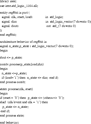
- The state process defines a storage element which is 8-bits wide, rising edge triggered, and
had a low true asynchronous reset.
- The output of this process is the p_state signal.
- Note that the reset input has precedence over the clock in order to define the
asynchronous operation.
- The 'event attribute is used to detect a change in the clock signal; comparing the
current clock value against '1' implies that p_state gets the n_state value
on a 0 to 1 transition (rising edge).
- The state holding action of the process arises from the fact that p_state is not
assigned a value is reset is not asserted and a rising clock edge does not occur.

BACK TO INDEX
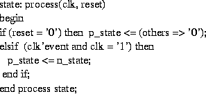
- An alternative method of specifying the storage elements is shown below:

- The wait statement is a sequential statement.
- The wait statement causes a suspension of a process or procedure until the condition clause is
satisfied.
- The signals used in the condition clause form an implicit sensitivity list for the wait statement.
- Can use 'wait on sig1, sig2, ..sigN until condition_clause' to explicitly specify the
sensitivity list.
- Note that the process has no sensitivity list.
- 'if' statements used with processes generally give more flexibility and control than 'wait'
statements .
BACK TO INDEX

BACK TO INDEX

BACK TO INDEX


BACK TO INDEX
- One-Hot encoding of FSMs uses one flip-flop per state.
- Only one flip-flop is allowed 'on' at anytime.
- E.G., states are "00001", "00010", "00100", "01000", "10000" for a five state FSM.
All other states are illegal.
- One-Hot encoding trades combinational logic for flip-flops.
- Good for 'flip-flop' rich implementation technologies.
- Because the combinational logic is reduced, the length of the critical path can be
reduced resulting in a faster FSM. Speed increase is more significant for larger
finite state machines.
BACK TO INDEX


BACK TO INDEX

BACK TO INDEX


BACK TO INDEX
- The 'for-loop' VHDL construct can be used to create a scan-path in your design.
A scan path is a design technique used for improving the testability of a design.
- A scan path requires three extra pins on the design: 'scan', 'scan_in',
and 'scan_out'.
- When 'scan' is asserted, all flip-flops in the design act like a serial shift register; the
'scan_in' pin is the serial input and the 'scan_out' pin the serial output. When
'scan' is negated the design functions normally.
- Because all flip-flops in the design are on the scan path the circuit can be placed
in any desired state.
- To enter a test vector via the scan path do:
- Assert 'scan'.
- Apply the test vector serially to the 'scan_in' input; this requires
N clocks if N flip-flops are on the scan path.
- Negate 'scan', clock the circuit once. This will allow the circuit to operate
normally for one clock cycle; the result of the test vector will be loaded into
the flip-flops.
- Assert 'scan'; clock N times to clock out the test vector result and to clock in
the next test vector. Thus, each test vector requires N+1 clocks.
BACK TO INDEX

BACK TO INDEX
- Add 'scan', 'scan_in' to port list. 'scan_out' will be MSB of port 'stateout'.
entity tlc_onehot_scan is port (
	signal reset, car, timer, clk : in std_logic;
	signal scan,scan_in : in std_logic;
	signal stateout : out std_logic_vector(4 downto 0);
	signal highway_light, farm_light:out std_logic_vector(4 downto 0);
	signal start_long_timer, start_short_timer : out std_logic
); end tlc_onehot_scan;
- Add 'scan', 'scan_in' to sensitivity list of process: state_machine.
state_machine : process (scan, scan_in, reset, car, timer, p_state)
BACK TO INDEX


BACK TO INDEX
